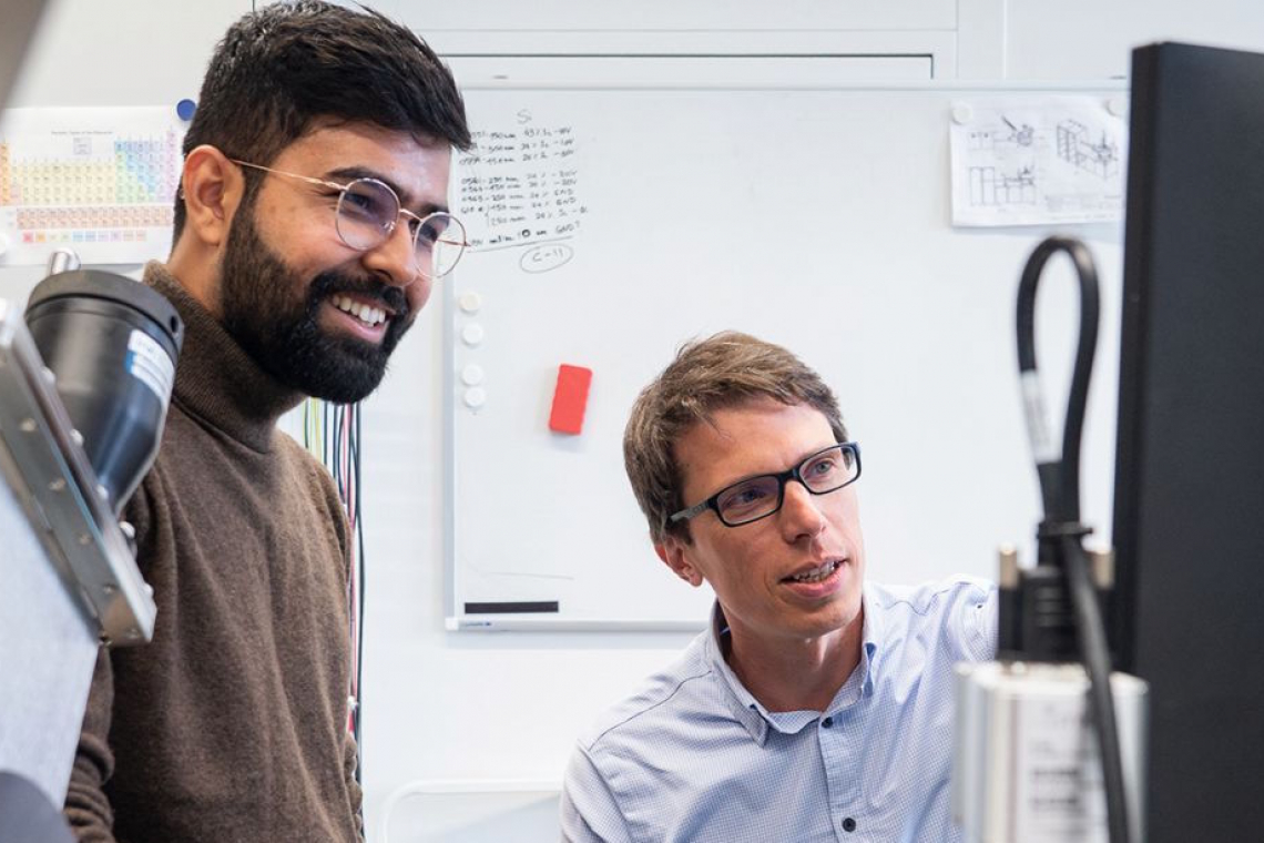
Empa researchers have developed a process for piezoelectric thin films in which sophisticated timing enables high-quality functional layers even on insulating substrates at low process temperatures. The basis is a modified HiPIMS (High Power Impulse Magnetron Sputtering) process. In order to avoid argon inclusions, it was possible to achieve clever timing of the voltage application so that the argon ions reach the surface more quickly and cannot anchor themselves to the substrate due to a lack of energy. The challenge of applying layers to electrically non-conductive substrates (glass or sapphire) was also solved: Each pulse of the magnetron automatically accelerates the negatively charged electrons. They arrive at their destination much faster than the ions. The "electron shower" causes the substrate to receive a negative charge for a fraction of a second, enough to accelerate ions. If the subsequent magnetron pulse is triggered at exactly the right time interval, the target ions that "flew off" during the previous pulse are accelerated. The researchers call this process "Synchronized Floating Potential HiPIMS", or SFP-HiPIMS for short. Applications are possible in the semiconductor industry and future quantum and photonics technologies.


