1 Introduction
It would be interesting to start this article with a quiz as follows:
What material is
- invisible (nearly transparent) to the human eye
- just about the lightest
- strongest on earth (200 times tougher than steel)
- thinner than a human hair (just one atom thick)
- characterized by largest surface area known for its weight
- stiffer than diamond and yet can be stretched by a quarter of its length like rubber, finally
- excellent conductor of heat and electricity?
All those above properties might sound like the stuff of science fiction, but believe it or not, such material exists. The name of this extra-ordinary material is graphene. The word graphene incidentally has come from a Greek word graphein meaning 'to write’ because in early days this word was used to write marking the sheep.
Science journals of graphene have been running out of superlatives for this wondrous stuff. If one believes in hype, graphene apparently promises to revolutionize everything from computing to car tires and solar cells to smoke detectors. Although not much to look at this single layer of carbon atoms that forms graphene, it, however, provides the most exciting prospects in science today. In fact, according to the experts, if the 20th century was the age of plastics, the 21st century seems set to become the age of graphenes which are simply sheets of carbon of one atom thick.
The extra-ordinary properties of graphene have led to overwhelming worldwide research of this material. As a result, vast amount of work published in the literature on graphene which may prove to be beyond the simple academic grasp of general readership. The intricacy of the theoretical treatment of grapheme is avoided in the present article. Instead, a comprehensive review of work on graphene is presented in the current article (Part 1) for an appreciation of this material based on a literature survey as well as comments of experts. In addition, a background history of development of materials in the ancient time is briefly highlighted to reflect my personal interest as an-ex student of metallurgy. In Part 2, property, production and application of graphene are discussed.
 Fig. 1: Writing with a normal pencil on paper is a kind of coating which can be compared with the coating of a flexible substrate with graphene
2 Highlighting the development of materials in ancient time
Over the past millennia, technological advances to a large extent have determined the course of civilization and even history. In fact, it is always risky to make broad assertions about history. However, one of the few things that seems to hold truth is that technological advances drive the course of civilization. Bronze and iron were so crucial in the history and development of ancient societies that they retrospectively have entire epochs named after them namely the bronze and iron ages. During the Bronze Age (≈3300-1200 BC) it was the production of the harder and more durable bronze through the smelting of copper and adding of tin or arsenic that gave civilizations a technological advantage. In the Iron Age (≈1200-600 BC), iron and steel were introduced and people started to make tools and weapons superior to their bronze equivalents. Iron tools made farming much easier, Superior iron weaponry were produced that allowed the Persians to establish the first Persian Empire as one of the largest empires in history, extending from the Balkans of Eastern Europe to the Indus Valley in India.
2.1 Brief consideration of subsequent progress
With the rise of the American steel industry, railroad tracks spread from Atlantic to Pacific can be described as metal veins that carried the blood of a nation by enhancing transport and trade. The rise of the Silicon semiconductors enabled the building of computers which is one of the greatest technological innovations since the Gutenberg printing press of 1450. All the technologies and materials thus involved moulded the development of society, and contributed to their global domination.
3 Historical development of graphene
Scientists have been puzzling over graphene for decades. Prior to its surprising discovery in 21st century (to be discussed later on), knowledge of graphene remained hidden since 1656 behind its source namely the pencil trace. Sporadic attempts to study graphene can be traced back to 1859. Back in 1947, Canadian physicist Philip Wallace wrote a pioneering theoretical paper on the electronic behaviour of graphite that sparked considerable interest in the field. He predicted the electronic structure and noted the linear dispersion relation. The wave equation for excitations was already established (Phys.Rev. Vol 104, 666 1956), and its similarity to the Dirac equation was discussed by G.W. Semenoff in 1984.
Nobel-Prize winning chemist Linus Pauling was speculating as long ago as 1960 about how flat, single layers of carbon atoms (such as graphene unknown at that time!) would behave! In 1962, such materials were named „graphene“ by German chemist Hanns-Peter Boehm, who had spotted them under his electron microscope the year before.
Theoretical research into graphene continued for the next four decades, boosted in the 1980s and 1990s by the discoveries of fullerenes (effectively, graphene curled up into balls) and carbon nanotubes (graphene folded into a pipe). Even so, no-one could ever actually make the stuff in practice; graphene was only produced in a laboratory in 2004 despite the fact that there has been an explosion of research on graphene in the 20th century.
The starting material for graphene was originally graphite which is the most stable form of carbon in nature that had been known for a long time – humans have been using it since the Neolithic era. Such a fact would obviously imply that graphene is not a new material but has always been there inside graphite. Its atomic structure is well documented, and for a long time, scientists pondered whether single layers of graphite could be isolated. Until recently, however, graphene was merely a theory because scientists were unsure if it would ever be possible to slice graphite down to a single, atom-thin sheet. However, developmment of a novel unusually playful ingenious method produced graphene in 2004.
4 Discovery of graphene
Statement such as “the aspects of things that are most important to us, are sometimes hidden because of their simplicity and familiarity” applies in the present case because of simplicity of discovery of graphene. Thus on one Friday in 2004, Russian-born scientists Professor Sir Andre Geim and Professor Sir Kostya Novoselov working at UK's University of Manchester, used a pencil (graphite) on a piece of sticky tape.
4.1 Background of the concept
Any pencil (Fig. 1) is typically a wooden shaft filled with a stick of soft graphite which is a type of carbon made from strongly bonded layers of atoms that are very weakly held together by the so-called van der Waals force. As the pencil is dragged along a page, thin layers of graphite shear off and stay behind on the paper displaying a black line as shown below. This could lead to producing graphene of just one atom high if only a super-thin layer of graphite of the pencil is shaved off. It would be worth mentioning here that there are many tiny specks of graphene are thus likely to be formed in any pencil line. However, since graphenes are only one atom high, it is almost impossible to spot them!
The most important ingredient in an ordinary pencil is always graphite, which most people continue to call lead. Conté's method of combining graphite with clay is still used, and wax or other chemicals are sometimes added as well. Virtually all graphite used today is a manufactured mixture of natural graphite and chemicals.
Here is a myth buster: There is no lead in pencils. Rather, the core is made up of a non-toxic mineral called graphite. The common name “pencil lead” is due to an historic association with the stylus made of lead in ancient Roman times.
Back to the work of Geim and Novoselov mentioned earlier. They pulled off some graphite flakes from the black line. These flakes thus originated from a chunk of the conventional bulk crystals of graphite (as used in a common wooden pencil), and were peeled off with the sticky tape. They noticed that some flakes were thinner than the others and were held together on the sticky tape by van der Waals forces. These fine flakes on the tape were next pulled off the tape, folded and pulled apart to cleave the graphite even into smaller layers. Eventually, after a great deal of patience/work, they were amazed to discover bits of extremely thin graphite (carbon) films which were thus obtained by separating the graphite fragments repeatedly. Thus by accidentally shaving off some flakes of graphite, graphene was discovered for the first time. It was a single layer of carbon of one atomic thick. As a result of the thickness of graphene being only a single carbon atom i. e. one atomic thick, it was almost impossible to see graphene with naked eyes. In fact, for this reason researchers have excuses to take so long to find graphene sheets among the thicker stacks of graphite.
Furthermore, according to the experts, although this one atom thick material had unknowingly been produced by humans since the 17th century, it is only recently, however, after more than 400 years, we were really able to study its properties closely. This material always had an economic appeal in the 17th century for the production of pencils. And now in the 21st century, it is apparently the best material of choice for high-end flexible electronics.
In fact, four years later after the discovery, the Manchester team managed to create a graphene transistor of just one atom thick and ten atoms wide. The same year, workers at Rice University in the United States built the first graphene-based flash memory. One forecast predicts that the graphene industry will be worth £ 300 bn. by 2022. Summarising the text so far: Graphene was discovered by simply peeling off super-thin layers of carbon as flakes from graphite of a pencil using a sticky tape (mechanical exfoliation method). There were, however, some upsets at the earlier stages of the discovery as explained in the next section. Nevertheless, one can conclude that graphene is the basic building block of all graphitic materials. Since the material found in pencil “lead” is graphite, any pencil used in drawing on a paper would provide weakly bound graphene sheets that originate from the graphite and spread over the paper like a pack of cards.
One would get the impression from above story of mechanical exfoliation that it is easy to make graphene. This is certainly not true. Thus, anyone with some scotch tape and a piece of graphite in a pencil could attempt to produce graphene. But such simple technique will if anything will only provide a small amount, and would not be easy to make a lot of graphene. Efforts are thus being made all over the world to develop various production routes for larger amount of graphene as discussed later on (A new five storey building of National Graphene Inst. where the original work was carried out, has been built in Manchester in 2015).
 Fig. 2: Typical sketches of a single layer of carbon atoms forming a planar hexagonal honeycomb lattice of graphene
5 Dimensional characteristics of graphene
Dimensional aspect of graphene is quiet intriguing. Any 'spatial’ description of a solid material on this planet would always include three parameters namely length (x), width(y) and height (z) i.e. has three dimensions (3D). In contrast, graphenes represent a conceptually new class of materials. They are only one atom thick and exist only in two dimensions: length and width while their third dimension namely height does not exist i.e. zero, making them two-dimensional (2D) materials.
Graphene can now be defined as a 2D material. It is a crystalline material of a single layer of carbon atoms laid out flat like billiard balls of one atom thick on a table. Each layer of graphene is densely packed on an atomic-scale in a regular hexagonal, honeycomb lattice resembling chicken wire structure of one atomic or molecular thick of crystals of carbon (Fig. 2).
Each carbon atom has four electrons in its external electronic layer and is connected to three other atoms,while the fourth electron is free on the surface of the network. It is the cumulative availability of these loosely connected electrons which are very mobile that make graphene an excellent conductor of electrical energy. Additionally, this one-atom-thickness makes graphene sheets transparent. The excellent properties of the material for optoelectronic applications are due to the combination of these two characteristics: conductivity and transparency.
For the enthusiasts, each carbon atom in graphene has four bonds, one σ bond with each of its three neighbours and one π-bond that is oriented out of plane. Its thickness is characterised by of one atom forming on each vortex. The extraordinary characteristics of graphene originate from the 2p orbitals, which form the π state bands that delocalize over the sheet of carbons that constitute graphene.
5.1 Initial set back of the pioneering work
The scientific world was very sceptical about Geim and Novoselov’s work. As a consequence, their original joint paper was initially rejected twice by the prestigious journal such as Nature. Scientists argued that strictly speaking any 2D crystalline material is thermodynamically unstable and therefore could not exist. However, it was only much later their paper on this remarkable, exciting material was approved for publication. Discovery of this unique material was eventually rewarded with a Nobel Prize for Physics to both Geim and Novoselov in 2010.
5.2 Several unusual facts about graphene
Being around million times thinner than a human hair, graphene is the thinnest object ever created. Furthermore, since the layers themselves are just one atom high i.e. 2D only, a stack of about three million of these layers would be needed to make 1mm thick graphene! Several sheets of them if stacked one on top of the other would be regarded as multi-layer graphene, and up to the point the material would becomes graphite (usually over about 30 layers, although clear standardization is severely lacking at the moment) which is found in pencils.
As a first 2D material, graphene captured the attention of scientists and researchers worldwide. The in-plane 2D carbon-carbon bonds in graphene provide the strongest bonds known to science. Such bonds give graphene its unbelievable mechanical strength and flexibility. Ironically, although ultra-light, it is yet immensely tough. It is fire resistant yet retains heat. It is a superb conductor, but not even helium can pass through it. While scientists have known graphene since 2004, it was not until 2010 when researchers from Samsung and Sungkyunkwan University took a critical step in developing the commercial applications of this material.
Despite the chemical bonds in the plane are very strong, the bonds between planes in graphene are extremely weak. As a result, the planes of carbon atoms can slide on top of each other. Each time a pencil is used, part of the graphite is transferred to the paper with the shear force moving several graphene layers inside the paper through the weak interlayer coupling. No single graphene sheet can be detected because each of them is highly transparent by being too thin to reflect light significantly. Furthermore, graphene is a crystalline allotrope of carbon in the form of a nearly transparent (to visible light) of one atom thick sheet.
6 Research prospects
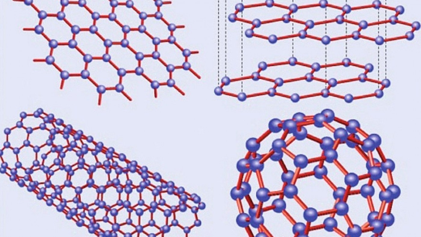
 top right: graphite = stacked graphene, 2) top left: graphene, 3) bottom right: fullerene = wrapped graphene and 4) bottom left: nanotube = rolled graphene") Fig. 3: Forms of graphitic matarials: 1) top right: graphite = stacked graphene, 2) top left: graphene, 3) bottom right: fullerene = wrapped graphene and 4) bottom left: nanotube = rolled grapheneThe combination of unusual properties of graphene was quickly recognized by the researchers of great interest. Rapidly emerging as a hugely promising material of 21st century, graphene has been widely researched, engineered and studied. Interestingly, every pencil mark contains a tiny speck of graphene, but since they are only one atom high, as mentioned earlier, we cannot see them.
Fig. 3: Forms of graphitic matarials: 1) top right: graphite = stacked graphene, 2) top left: graphene, 3) bottom right: fullerene = wrapped graphene and 4) bottom left: nanotube = rolled grapheneThe combination of unusual properties of graphene was quickly recognized by the researchers of great interest. Rapidly emerging as a hugely promising material of 21st century, graphene has been widely researched, engineered and studied. Interestingly, every pencil mark contains a tiny speck of graphene, but since they are only one atom high, as mentioned earlier, we cannot see them.
Carbon atoms come in various crystallographic forms i. e. allotropes which range from graphite found in the pencils to the world's most expensive item namely diamonds. The three basic crystalline forms i.e. allotropes of carbon are diamond, graphite, and amorphous carbon were known by 1980. Later on fullerenes (which is graphene curled up into balls) and carbon nanotubes (graphene folded into a pipe) were discovered and in 2004, graphene joined the club.
Boosted in the 1980s and 1990s by the discoveries of the varieties of forms of graphitic materials, theoretical research continued for the next four decades of the following shaped materials (Fig. 3) which are descendants of graphene [C. Neto; F. Guinea; N.M.R. Peres: Drawing conclusions from graphene, PhysicsWorld, Vol 19, 2006, 33].
With so many varieties of graphene being available, it had been relatively simple for the researchers to move from an area that was scientifically saturated to a new one with minimal amount of investment in terms of resources and, especially, time.
7 Future of graphene
According to the experts, production issues aside, graphene research is by no means slowing down. Research laboratories over the world are continually filing patents for new methods of creating and using graphene.
The European Union approved funding for a flagship program in 2013, one that will fund graphene research for use in electronics. Perhaps more importantly, many major tech companies in Asia are conducting research on graphene, including Samsung. As the EU tries to steady its footing in the face of explosive economic growth in Asia, graphene could be an important battlefield in international politics in the coming years.
Graphene can act as sensors via its high detection power that can detect even minute traces of gases or dangerous chemicals, or sustainable food packaging that can let one know when food has gone off. This material absorbs light and retains it as energy. Besides its strength and flexibility, graphenes are getting closer to enormous battery life for wearable electronics and clothing that communicate bendable mobile phones and cameras. Such future technologies are becoming realistic in near future. With low weight and high strength, harnessed with polymers and composites graphene could make numerous forms of transport safer and more fuel efficient. Source: http://www.graphene.manchester.ac.uk.
Currently graphene sells for $100 to $200 a gram but the market is counted in terms of kilograms. That size of the market is projected to increase rapidly once graphene is industrially produced. Soon the graphene market is expected to be real and significant.
8 Final comments
Graphene has the potential to change the future as in the case of history in the past. It could very much be the technology that changes the course of history in the 21st Century. Scientists are continuing to work out ways to harness usefulness of graphene in a way that would ensure a healthy profit for the investors.
It is quite likely that the remarkable characteristics of this 21st Century technological marvel could have far-reaching implications for the future of physics, engineering, bioengineering and civilisation as a whole. According to the exerts, no other material has the same breadth of properties that graphene boasts, making it ideal for countless applications. This would make graphene the object of research by scientists in fields varying from consumer technology to environmental science. Particularly in transport, medicine, electronics, energy, defence, and desalination, to name a few, graphene research is reported to be making a substantial impact.
It seems as if the potential of graphene is limited only by our imagination. However, despite its frenzy of progress, many researchers are cautious. Some are certain that graphene will not do everything that has been thought up for it. What has been reported as „potential“ seems to be live at the moment – just that along with few real-world examples of it working to replace other materials.
Question we ask: “is it full-steam ahead to a future when graphene will rule the world?” Maybe or maybe not. It's important not to get carried away with the hype: we ought to remind ourselves that most of the exciting work on graphene has so far been done on a very small scale in the laboratories. -to be continued-