1 Introduction
 Fig. 1The basic factors influencing the development of graphene had been considered in Part 1. Parameters such as property, production and applications of graphene are discussed in this Part 2 of the present text. This new material graphene is tougher than a diamond yet more elastic than rubber, 100–300 times stronger than steel. To put this into perspective: if a sheet of cling film (like kitchen wrap film) had the same strength as a pristine monolayer of graphene, it would require the force exerted by a mass of 2000 kg, or a large car, to puncture it with a pencil. It is also lighter than aluminium and thinner than a flea’s hair (1sq.meter area will weigh only around 0.1 milligrams). Such an array of properties would provide graphene with very promising potential applications in a variety of technological fields to be discussed later on.
Definition of graphene is that it consists of a single, thin layer of graphite which is the soft, flaky material used in pencil lead. A typical pencil shown below (Fig. 1) is a wooden shaft filled with a stick of soft graphite, a type of carbon made from strongly bonded layers of atoms that are very weakly held together by van der Waals forces. When one drags the pencil along the page, thin layers of graphite shear off and stay behind, making a black line which one can see. Now if during this activity, one could shave off a super-thin layer of graphite of just one atom high, the material that would be left with is 'graphene’. With this experience, one can no doubt expect some tiny specks of graphene being always left over on a piece of paper whenever a pencil mark is made as shown above. However, since graphenes are only one atom high, it will be almost impossible to spot them with naked eyes!
Dubbed as “super material,” graphene has researchers all over the world scrambling for a better understanding of it. The long list of superlative traits of graphene (Part 1) makes it almost appearing to be magical – it has the potential to alter the future with very possible real and drastic implications for the prospect of physics and engineering. The range of properties and production routes are described here in Part 2 along with some definite as well as speculative applications.
2 Basic difference between Graphite and Graphene
Graphene is the building block for graphitic materials. It is worth pointing out at this juncture that the major difference between graphene and graphite is that graphene is only a mono-layer of graphite – one can expect to produce nothing but bulk graphene and graphite in the end by stacking together a bunch of graphene. The following few properties of graphene will basically differentiate it from graphite:
- graphene has high electron mobility therefore, high electrical conductivity (isolated graphene has 106 cm2/V.s)
- graphene has zero Energy Bandgap
- graphene has High tensile strength (Strongest material ever discovered).
It is worth reiterating that if graphenes are stacked up on top of one another, they could theoretically re-form the parent material i.e graphite which is found in every pencil lead. In fact anyone who has drawn a line with a pencil has probably made multiple hexagonal carbon networks of graphene. With carbon atom having a diameter of about 0.33 nanometers, there will be typically about 3 million layers of graphene in 1 mm of graphite.
3 Properties of graphene
3.1 General considerations
As a vitally important parameter, properties are considered in some details. Such a discussion will help one to appreciate the wide variety of applications of graphene.
Some of the amazing characteristics of graphene include:
- despite being the thinnest material known in the world, it is surprisingly also one of the strongest materials
- conducts heat 2x better than diamond
- it absorbs only 2.3% of reflecting light
- it is almost completely transparent but dense, impervious/impermeable to gases or liquids that even the smallest atom (such as helium) cannot pass through a defect-free monolayer of graphene sheet. This unusual combination of properties, and the fact graphene is nearly invisible, makes it an ideal material for the transparent electrodes used in computer displays and solar cells
- its high surface area of 2630 square meters per gram means that with less than 3 grams one could cover an entire soccer field (well, practically speaking one would need 6 grams, since 2630 m2/g is the surface area for both sides of a graphene sheet).
 Fig. 2A summary of typical set of properties of graphene is presented below (Fig. 2).
Electrons flow through graphene with almost zero electrical resistance and is thus an excellent/better conductor of electricity and conducts electricity as efficiently as copper while outperforming other materials as a conductor of heat. It can be made into transistors which are faster than those made from silicon. Its high electron mobility is 100 xs faster than silicon.
Many other distinctive characteristics besides those already been mentioned above, include thermal (the best conductor of heat at room temperature) and electrically conductivity, while still transparent. It is magnetic, has a uniform absorption of light across the visible as well as near-infrared parts of the spectrum, and apparently impermeable to most liquids and gases. Above all, since carbon is the basis for all known life on earth (2nd most abundant mass within the human body and the 4th most abundant element in universe), graphene which is only constituted of carbon, is an eco-friendly, and a sustainable solution for an almost infinite number of applications.
3.2 Mechanical properties
The impressive intrinsic mechanical properties of grapheme include its stiffness, strength and toughness, are one of the reasons that make graphene stand out both as an individual material and also as a reinforcing agent in composites. They are caused by the stability of the sp2 bonds that form the hexagonal lattice and oppose a variety of in-plane deformations
Strength
Defect-free, monolayer graphene is considered to be the strongest material ever tested with a strength of 42 N m-1 that equates to an intrinsic strength of 130 GPA.
Toughness
Fracture toughness, which is a property very relevant to engineering applications, is one of the most important mechanical properties of graphene and was measured as a critical stress intensity factor of 4.0 ±0.6 MPa.
Research groups worldwide are working on the development of industrially manufacturable graphene sheets that have high strength and toughness in all sheet directions for diverse applications of graphene-based composites for vehicles, optoelectronics and neural implants.
3.3 Allotropes of carbon (descendents of graphene)
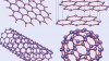
Allotropes by definition are the same material as the parent i.e. with the same atomic weight, but are of different configuration. With carbon, scientists have discovered several allotropes in the last few years. They include fullerenes, (discovered in 1985; hollow cages of carbon atoms, including the so-called Buckyball, Buckminsterfullerene made from a kind of football-shaped cage of 60 carbon atoms) and carbon nanotube (discovered in 1991; flat sheets of carbon atoms curled into amazingly thin, hollow tubes one nanometre in diameter) – and finally graphene (discovered in 2004).
 Fig. 3
3.3.1 Allotropic structures of graphite, diamond and graphene
Although diamonds and graphite are both made of identical carbon atoms, their characteristics are radically different since the atoms are arranged in completely different ways. In diamonds, the atoms are tightly bonded in three-dimensional tetrahedrons (or as triangular pyramids), whereas in graphite, atoms are bonded tightly in two-dimensional layers held together by weak forces compared with the two dimensional configurations of graphene. The specific arrangements of atoms in diamond and graphite give the two materials their different properties: graphite is black, dull and relatively soft while diamond is transparent as well as one of the hardest natural materials.
In Figure 3, sketches of diamond, graphite and graphene are presented followed by various allotropes mentioned above as descendants of graphene [Castro Neto; F. Guinea; N.M.R. Peres: Drawing conclusions from graphene, PhysicsWorld, Vol 19, 2006, 33].
- Diamond has a strong 3D (three-dimensional) crystal lattice based on a repeating tetrahedron (left). The red blobs are the carbon atoms and the gray lines are the bonds that join them together. Bonds are invisible, but are drawn them like this so one can visualize them more easily.
- Graphite has a much weaker structure based on layers of tightly bonded hexagons. The layers are weakly joined to one another by van der Waals forces (blue dotted lines – only a few of which are shown for clarity).
- Graphene has a flat crystal lattice made from interlinked hexagons of carbon atoms (red blobs) tightly bonded together (black lines).
Following sketches (reproduced from Part 1) are displayed to represent:
- top right: graphene;
- top left: graphite = stacked graphene;
- bottom right: fullerene = wrapped graphene, and
- bottom left: nanotube = rolled graphene where graphene has the same structure of carbon atoms linked in hexagonal shapes to form carbon nanotubes, but it is flat rather than cylindrical (Fig. 4).
3.3.2 Selective properties of carbon allotropes
Graphene possesses not only unique electronic properties, but also excellent mechanical, optical, thermal and electrochemical properties that are superior to other carbon allotropes. Graphene’s superior properties are summarized in Table 1 [1–6].
| Carbon allotropes | Graphite | Diamond |
Fullerene (C60) |
Carbon nanotube |
Graphene |
| Hybridized form |
sp2 |
sp3 |
Mainly sp2 |
Mainly sp2 |
sp2 |
| Crystal system | Hexagonal | Octahedral | Tetragonal | Icosahedral | Hexagonal |
| Dimension | Three | Three | Zero | One | Two |
|
Experimental specific surface area (m2 g-1) |
~10–20 |
20–160 | 80–90 | –1300 |
~1500 |
|
Density (g cm-3) |
2.09–2.23 | 3.5–3.53 | 1.72 | >1 | >1 |
| Optical properties | Uniaxial | Isotropic |
Non-linear optical response |
Structure- dependent properties |
97.7 % of optical transmittance |
|
Thermal conductivity (W m-1 K-1) |
1500–2000a, 5-10c |
900–2320 | 0.4 | 3500 | 4840–5300 |
| Hardness | High | Ultrahigh | High | High |
Highest (single layer) |
| Tenacity |
Flexible nonelastic |
– | Elastic | Flexible elastic | Flexible elastic |
| Electronic properties |
Electrical conductor |
Insulator, semiconductor |
Insulator | Metallic and semiconduction |
Semimetal, zero-gap semiconductor |
|
Electrical conductivity (5 cm-1) |
Anisotropic, 2–3 x 10⁴a, 6b |
– |
10-10 |
Structure- dependent |
2000 |
3.4 Properties of graphene nanotube as a special case
Graphene/carbon nanotubes (Fig. 5) are made of a 2D matrix of carbon-carbon bonds formed into cylinders. This means they can bend and twist without breaking bonds, and along that trend of thought they cannot stretch very far before bonds are broken. These nanotubes are strong because they constitute a single chain of unbroken covalent carbon-carbon bonds.
More than that, they have many carbon-carbon bonds at each step, so breaking a carbon nanotube requires breaking many strong covalent bonds. A diamond, for example, is so hard because it is a 3D matrix of carbon-carbon bonds – if it deforms in any way, bonds have to be broken which is not an easy proposition. Thus they would be highly resistant to extension beyond a certain point. And that is what meant when one says they are strong.
3.5 EU in the lead
Over the next 10 years the EU will invest €1 billion in developing graphene-based technologies through the Graphene Flagship initiative, which is part of the Horizon 2020 programme. The aim is to develop graphene and related layered materials into something that can be used for everyday products. Graphine makes it possible to conduct experiments with high-speed quantum particles that researchers at CERN near Geneva, Switzerland can only dream of.
4 Production of graphene
 Fig. 4In their initial experiments, Geim and Novoselov recovered graphene from a piece of graphite such as is found in ordinary pencils using an adhesive tape. They managed to obtain flakes of carbon with a thickness of just one atom. This process of mechanical exfoliation is the simplest method of preparation. It was quite obvious from the very beginning that such method suffers from the big limitation of not being suitable for mass applications. Thus development of a mass production method was badly needed. In fact, even before 2004, many researchers were working on the growth of graphene by artificial means. The growth out of SiC (silicon carbide) as a base, for instance, is considered one of most promising ways of producing large area graphene for electronic applications.
The most common techniques available today include chemical vapour deposition (CVD), chemical reduction of exfoliated graphene oxide, micromechanical cleavage, epitaxial growth on SiC substrates, liquid phase exfoliation (LPE) of graphite and unzipping of carbon nanotubes. Amongst these alternative techniques, the most popular method of making graphene has been the CVD technique which involves a mix of gases reacting with a surface to create a graphene layer. The process creates high-quality graphene which, however, is often damaged when it comes time to detach it from its substrate. However, the technique has recently become more popular because of its simplicity and low cost (and possibly its interesting environmental impact namely ability to capture CO2 for graphene production). Researchers have already managed to produce large, single-crystal-like graphene films more than a foot long on virtually any flat surface – a step towards commercialization.
It should be emphasized that, currently, only the chemical reduction of exfoliated graphene oxide i.e. chemical exfoliation method is considered as a common route toward the production of graphene at low cost and in a large quantity [7]. It first involves oxidation of well-stacked graphite to graphite oxide (GO) [8], and followed by chemical reduction of GO to obtain reduced GO (rGO) [9] or thermal exfoliation of graphite oxide [10–13] to produce graphene. However, each of these methods has its own advantages as well as limitations depending on the target applications. The global graphene production appears to suffer from the following serious quality issues (see Sec. 4a below), and it appears that there is almost no high quality graphene, as defined by ISO, in the market yet.
4.1 Possible production problems
Organisations intend to produce graphene, have to be aware of the following problems:
- strong interaction with the substrate can lead to large charge transfer and difficulties in transferring the material to an appropriate (flexible) substrate. Mechanical stability during the transfer process to plastic (for flexible electronics) can lead to structural failure
- formation of extended defects due to heterogeneous growth can reduce the electronic mobility
- by using the adhesive tape method i.e. mechanical exfoliation and transferring graphene to a silicon wafer, it is possible to produce a very small amount of graphene; however, the material’s myriad applications “require more than a tiny flake of graphene, and scaling up production requires something other than a really big piece of scotch tape”
- since the quality of graphene plays a crucial role for its electronic and optical properties, presence of defects, impurities, grain boundaries, multiple domains, structural disorders or wrinkles in the graphene sheet would adversely affect the quality
- furthermore, the major bottleneck in electronic applications is the requirement of large samples which is possible only in the case of CVD process. However, it is difficult to produce high quality and single crystalline graphene thin films by CVD possess that would provide very high electrical and thermal conductivities along with excellent optical transparency and
- finally, one more issue of concern in the synthesis of graphene by conventional methods involves the use of toxic chemicals. Most of the production methods usually result in the generation of hazardous waste and poisonous gases. Therefore, developments of green methods are urgently needed to produce graphene by adopting environmentally friendly approaches.
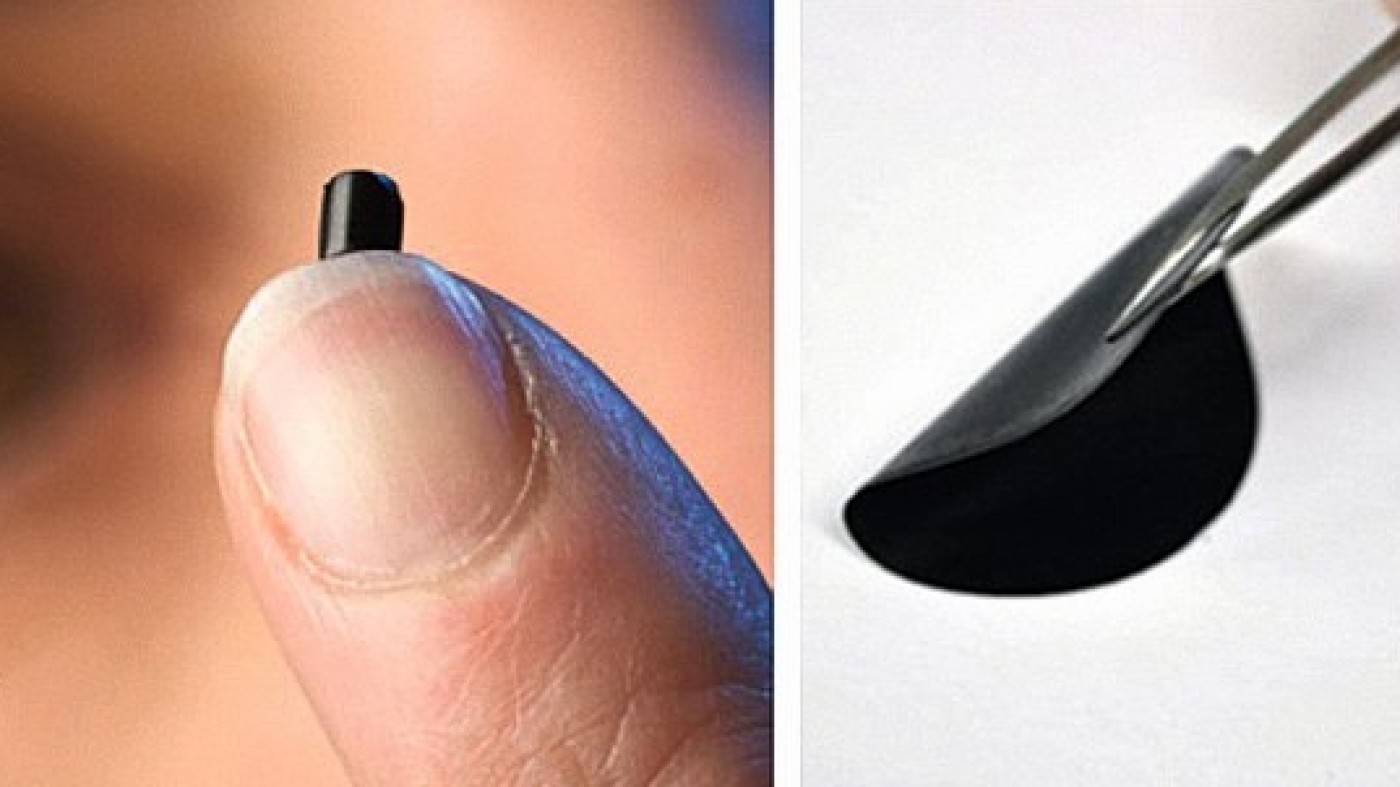
 and a foil (right)") Fig. 5: Carbon nanotube of one atom thick sheet of graphene, rolled into a cylindrical form (left) and a foil (right)In order to surmount the above barriers, concerted efforts are being made in commercializing graphene by researchers at various R&D institutes, universities and companies from all over the globe to develop new methods for large scale production of high quality graphene via simple and eco-friendly approaches but at low-cost. Only time and investment can tell which of the production method will be dominant for the industrial use of graphene. The fact of the matter is that today it is possible to produce large area graphene (even square meters) using CVD with reasonable electronic mobility (> 5,000 cm2/Vs). Hence, it is clear that the barrier for large area production has been broken. This is not to say that much development is still needed to make the material of the highest quality (single crystal) given that the CVD growth is heterogeneous and produces polycrystalline samples.
Fig. 5: Carbon nanotube of one atom thick sheet of graphene, rolled into a cylindrical form (left) and a foil (right)In order to surmount the above barriers, concerted efforts are being made in commercializing graphene by researchers at various R&D institutes, universities and companies from all over the globe to develop new methods for large scale production of high quality graphene via simple and eco-friendly approaches but at low-cost. Only time and investment can tell which of the production method will be dominant for the industrial use of graphene. The fact of the matter is that today it is possible to produce large area graphene (even square meters) using CVD with reasonable electronic mobility (> 5,000 cm2/Vs). Hence, it is clear that the barrier for large area production has been broken. This is not to say that much development is still needed to make the material of the highest quality (single crystal) given that the CVD growth is heterogeneous and produces polycrystalline samples.
It is worth mentioning that the preparation methods for graphene should allow for in-situ fabrication and integration of graphene-based devices with complex architecture – this laborious fabrication methods would result in lower production cost by eliminating the multi step (read more: “Mass production of high quality graphene: An analysis of worldwide patents”). Presently, Samsung has been one of the biggest investors in research in collaboration with South Korean Sungkyunkwan University. It has already demonstrated producing a 25-inch flexible touch screen using graphene.
Currently graphene sells for \(100 to \)200 a gram but the market is counted in terms of kilograms. That size of the market is projected to increase rapidly as graphene is industrially produced. However, neither the weight nor size is guaranteed. Also, the following questions need answers namely what is the profit in making graphene and what is the market size.
4.2 Commercial prospects
Profitability
It is important to recognize that graphene production techniques and processes are in public domain. This means that no company or, no select group of companies, is going to dominate the market through trade secrets and patents although they could overcome this via control of the resources that make graphene.
Expensive production
Scientists produce graphene 100 times cheaper than ever before. To produce high-quality material scaled-up for applications in electronics on large areas, graphene has, however, proved more expensive than standard electronic substrates such as silicon. A large part of the expense relates to the substrate on which Graphene is generally produced as revealed in an article on 22 Nov. 2015.
5 Applications
The applications of graphene and the applications of silicon are in different domains. With an array of properties, graphene makes it suitable for diverse applications ranging from electronics to optics, sensors, bio devices and lubrication.
Electronics applications
Graphene has a unique combination of properties that is ideal for next-generation electronics, including mechanical flexibility, high electrical conductivity, and chemical stability. Combining this with inkjet printing, one would get an inexpensive and scalable path for exploiting these properties in real-world technologies („Inkjet printing of graphene for flexible electronics“).
Corrosion resistance
Graphene is the world's thinnest known coating for protecting metals against corrosion. It was found that graphene, whether made directly on copper or nickel or transferred onto another metal provides protection against corrosion.
Sensor applications
Functionalized graphene holds exceptional promise for biological and chemical sensors.
Biotechnology and medicine
Recent research also points to an opportunity to replacing antibiotics with graphene-based photo thermal agents to trap and kill bacteria.
Lubrication
An important considerations in applying a solid lubricant at the micro- and nanoscale is the thickness of the lubricant and the compatibility of the lubricant deposition process with the target product. Graphene, with its atomically thin and strong structural with low surface energy, is a good candidate for these applications (“Graphene – the thinnest solid lubricant”). A selective range of applications of graphene as quoted in the literature is displayed in Figure 6.
 Fig. 6
Based on multi functionality of graphene, its research has resulted in about 10,000 scientific papers being published every year on a wide range of topics. There are high hopes about what might be accomplished with graphene in a wide variety of applications such as water filtration, game changer in electronics, energy generation, automotive, aerospace, healthcare, photovoltaics, semiconductors, electrodes to name a few.
5.1 One typical example – Filtration of water
Based on impermeability of gas through graphen, water purification as detailed below is an interesting one demonstrating utilisation of the unique properties of graphene.
Graphene’s tight atomic bonds make it impermeable for nearly all gasses and liquids. Curiously, water molecules are an exception. Because water can evaporate through graphene while most other gasses and liquids cannot, graphene could be an exceptional tool for filtration. Researchers at the University of Manchester tested graphene’s permeability with alcohol, and were able to distil very strong samples of spirits, as only the water in the samples was able to pass through graphene.
Of course, graphene’s use as a filter has potential beyond distilling stronger spirits. It could thus be immensely helpful in purifying water of toxins or radioactive materials such as uranium and plutonium present in water, leaving the liquid free of contaminants – thanks to graphene.
Speculative implication
As overpopulation continues to be one of the world’s most pressing environmental concerns, maintaining clean water supplies will only become more important. Indeed, record shows water scarcity afflicting more than a billion people worldwide, a number that will only continue to rise given current trends. Graphene filters have immense potential to improve water purification, increasing the amount of fresh water available. In fact, Lockheed Martin recently developed a graphene filter called “Perforene,”, which the company claims could revolutionise the desalination process.
6 Final comments
Any comment on graphene as a new unique material is likely to come up as fuss/excitement. If, for example, one considers the 20th century as the age of plastics, the 21st century seems structurally set to become the age of “graphene”. Typically it is arranged in a honeycomb configuration of carbon atoms of just a single layer of one atom thick.
Science journals have been running out of superlatives for this wondrous stuff. It is not only the lightest, strongest, thinnest material known to mankind, but also the best heat- and electricity conducting material ever discovered. This unique material is tougher than a diamond but thinner than a flea’s hair, and thus exhibiting this extreme range of properties, graphene has the potential to revolutionise the world. It can be used for everything from creating a bendy mobile phone screen to strengthening the wings of a jumbo jet.
It is obvious that one now would ask “if graphene is such a wonderful material, why do we not find it everywhere?” Well, this is often the case with new materials, namely graphene presently is still extremely expensive to produce in large quantities. As a consequence, its use is limited for any product at the moment that would demand mass production.
Despite the frenzy of progress, investment and press attention, many researchers are cautious. Some are certain that graphene will not do everything that has been thought up for the material. As mentioned in Part 1, revolutions do not happen overnight. Silicon was discovered in the mid-19th century, but it took nearly a century before silicon semiconductors paved the way for the rise of computers. Graphene, with its almost mythical qualities, might be the resource to drive the next era of human history. Only time will tell
Literatur
[1] A.K. Geim; K.S. Novoselov: Nature Materials 6 (2007) 183–191
[2] A.K. Geim: Science324 (2009) 1530–1534
[3] S. Pisana; M. Lazzeri; C. Casiraghi; K.S. Novoselov; A.K. Geim; A.C. Ferrari; F. Mauri: Nature Materials 6 (2007) 198–201
[4] F. Schedin; A.K. Geim;, S.V.Morozov; E.W. Hill; P. Blake; M.I. Katsnelson; K.S. Novoselov; Nature Materials 6 (2007) 652–655
[5] R.R. Nair; P. Blake; A.N. Grigorenko; K.S. Novoselov; T.J. Booth; T. Stauber; N.M.R. Peres; A.K. Geim: Science 320 (2008) 1308–1308
[6] C.N.R. Rao; A.K. Sood; K.S. Subrahmanyam; A. Govindaraj: Angewandte Chemie International Edition 48 (2009) 7752–7777
[7] S. Park; R.S. Ruoff: Nature Nanotechnology 4 (2009) 217–224
[8] W. Hummers; R. Offman: Journal of the American Chemical Society 80 (1958) 1339
[9] S. Stankovich; D.A. Dikin; R.D. Piner; K.A. Kohlhaas; A. Kleinhammes; Y. Jia; Y. Wu; S.T. Nguyen; R.S. Ruoff: Carbon 45 (2007) 1558–1565
[10] H.C. Schniepp; J.L. Li; M.J. McAllister; H. Sai; M. Herrera-Alonso; D.H. Adamson; R.K. Prud’homme; R. Car; D.A. Saville; I.A. Aksay: The Journal of Physical Chemistry B 110 (2006) 8535–8539
[11] M.J. McAllister; J.L. Lio; D.H. Adamson; H.C. Schniepp; A.A. Abdala; J. Liu; M. Herrera-Alonso; D.L. Milius; R. Caro; R.K. Prud’homme; I.A. Aksay: Chemistry of Materials 19 (2007) 4396–4404
[12] Z.S. Wu; W. Ren; L. Gao; B. Liu; C. Jiang; H.M. Cheng; Carbon 47 (2009) 493–499
[13] Z.S. Wu; W. Ren; L. Gao; J. Zhao; Z. Chen; B. Liu; D. Tang; B. Yu; C. Jiang; H.M. Cheng: ACS Nano 3 (2009) 411–417