Introduction
Due to its unique properties, tetrahedral amorphous carbon (ta-C) coatings have gained increasing interest in scientific research and in industrial applications. A sp3 bonded carbon fraction of up to 85 % [1–4] leads to its diamond-like characteristics with respect to chemical inertness, low friction coefficients, extraordinary high wear resistance and hardness up to 70 GPa. Thin ta-C films are therefore a very competitive solution for protective coatings and cutting-tool applications. Furthermore, their mechanical, tribological and electrical properties can be considerably modified by doping them with metals or nonmetals. Doping thin ta-C films with boron (B) can significantly reduce the intrinsic stress of the coating while maintaining the sp3 content at a constant high level [5, 6]. Also the electric conductivity at room temperature is increased by 5 orders of magnitude at a boron ratio between 0–8 at. % [2]. Silicon (Si) as a dopant was used to increase the thermal stability and adhesion of ta-C [7, 8]. Metals like iron (Fe) and molybdenum (Mo) change the structure of the coatings to a more graphitic-like carbon coating but also help to improve tribological properties, reduce intrinsic stress and electrical resistivity [9–12]. Doped carbon coating composites are used e.g. in electronics, micro electro mechanical systems, sensors and functional coatings of bipolar plates in PEM [12].
The buildup of dense ta-C structures with a high sp3 bonding fraction can be realized by specific PVD processes. One of the major requirements is to ensure that the impinging carbon ions have a certain range of energy of ~100 eV to induce the sp3 bonding in the growing film [3, 4].
However, arc-PVD methods suffer from the fundamental drawback of emitting a considerably high amount of carbon macro particles into the plasma during the evaporation process [3, 13, 14]. The incorporation of these particles into the growing film creates growth defects within the ta-C structure. These defects affect the mechanical, tribological, and optical properties of the coating by reducing hardness and increasing the surface roughness [13]. Additional plasma-filtering units, applying (electro-) magnetic fields, can be utilized to separate and remove particles by deflecting the cathodic arc plasma [3, 15] out of the line of sight. However, this is always associated with some reduction in deposition rates, hence slowing down the film growth. Post treatments on coatings are also an established method to smoothen the coatings [3, 16]. Another approach to reduce the surface roughening of PVD deposited coatings is to limit the particle emission from the cathode-material itself. This can be realized by regulating the deposition parameters but also by adapted cathode processes. Recent studies have shown that a combination of a filtered cathodic vacuum arc and the injection of silicon-containing trimethylsilane gas can significantly reduce the number of particles incorporated in the film [8].
In the present work the influence of metallic (Mo, Fe) and non-metallic (Si, B) doping elements on the surface properties of ta-C coatings was investigated using a method for analyzing the surface defect fraction of those deposited coatings. For this purpose the coatings were prepared by Laser Arc deposition [17] developed at Fraunhofer IWS Dresden, using not only pure carbon targets but also composite carbon cathodes (see Sec. 2). In addition to surface analysis, the hardness and Young’s modulus of the doped coatings were evaluated in comparison to pure ta-C.
Origin of growth defects
The aforementioned emission of macro particles in arc PVD processes is particularly pronounced for ta-C coatings due to a low mobility of the arcing spot on graphitic cathodes. The application of arc evaporation, leads to extreme temperature and pressure gradients within the target material near the cathode spot [3]. Irregular shaped carbon particles are broken off by thermo-mechanical shock effect and moved towards the substrate [3].
The macro particles are about few nm up to some μm in dimension and remain in solid state, due to the high melting point of carbon. Though only a minor part of the impinging carbon particles exhibit sufficient kinetic energy to be incorporated into the growing film, these particles significantly enhance the non-uniformity of the ta-C structure. By the continuous deposition of the growing film, these particles are localized imperfections in the film microstructure acting like seeds for so called nodular defects.
Furthermore, despite chemical-mechanical substrate pretreatment prior to deposition, including grinding, polishing, and substrate ion etching, it is technically impossible to achieve a perfectly smooth surface.
On the resulting topographical irregularities on the surface and the carbon particles further deposition leads to growth of the initial punctual defect into nodular defects, due to shadowing effects.
Figure 1 (left) shows a single growth defect initiated by a particle (seed). The irregular geometrical structure of the seed causes an unevenly distributed vapor flux in its surrounding area, with the result that some substrate parts are not coated at all. With continuous deposition this effect will cause a conical or spherical growing nodule, with a sharp transition area between the coating above the seed and the undisturbed surrounding coating matrix. In this area strong columnar growth and the formation of pinholes, and fissures can be observed, so that the nodules are often only weakly incorporated into the growing film. Thus, already at medium mechanical stress these nodules can be detached from the surface leaving open pores, and holes behind. These in turn are susceptible for oxidation processes, and can act as starting points for a delamination of the coating.
![Fig. 1: SEM-image of particle initiated defect growth, made visible by a repeated interruption of ta-C growth and the deposition of thin chromium marker layers (left); homogeneous ta-C films with grown defects causing a rough coating surface (right); both [3]](/images/stories/Abo-2022-03/gt-2022-03-0023.jpg "Fig. 1: SEM-image of particle initiated defect growth, made visible by a repeated interruption of ta-C growth and the deposition of thin chromium marker layers (left); homogeneous ta-C films with grown defects causing a rough coating surface (right); both [3]") Fig. 1: SEM-image of particle initiated defect growth, made visible by a repeated interruption of ta-C growth and the deposition of thin chromium marker layers (left); homogeneous ta-C films with grown defects causing a rough coating surface (right); both [3]
Fig. 1: SEM-image of particle initiated defect growth, made visible by a repeated interruption of ta-C growth and the deposition of thin chromium marker layers (left); homogeneous ta-C films with grown defects causing a rough coating surface (right); both [3]
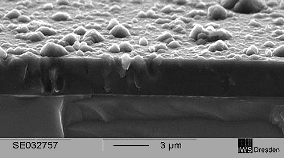
On the surface the growth defects will appear as dome- shaped hillocks, as shown in Figure 1 (right). The size and shape of these nodular defects are strongly influenced by the size distribution of the incoming plasma flux. Depending on the angle of incidence of the incoming ions, different cross-section geometries of the defects are possible. At a random vapor flux with a broad range of deposition angles a parabolic profile is formed, while narrow angular deposition will rather lead to defects having a conical cross section with straight sides. At stationary deposition angles these nodules can also be tilt in one certain direction as demonstrated in Figure 2 [18].
![Fig. 2: Scheme of a particle-induced growing defect with conical nodule cross-section due to stationary vapor flux; the shape mainly depends on the angle of incidence of the incoming ions: a) tilt 0°; b) tilt 45° [18]](/images/stories/Abo-2022-03/gt-2022-03-0025.jpg "Fig. 2: Scheme of a particle-induced growing defect with conical nodule cross-section due to stationary vapor flux; the shape mainly depends on the angle of incidence of the incoming ions: a) tilt 0°; b) tilt 45° [18]") Fig. 2: Scheme of a particle-induced growing defect with conical nodule cross-section due to stationary vapor flux; the shape mainly depends on the angle of incidence of the incoming ions: a) tilt 0°; b) tilt 45° [18]
Fig. 2: Scheme of a particle-induced growing defect with conical nodule cross-section due to stationary vapor flux; the shape mainly depends on the angle of incidence of the incoming ions: a) tilt 0°; b) tilt 45° [18]
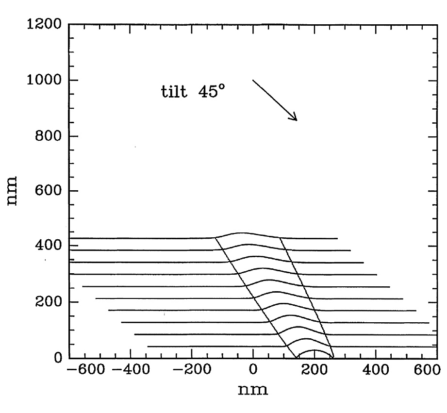
As a result of this parabolic or cone-like growth the lateral dimensions of the defects increase with growing film thickness and can significantly exceed the size of the initial seeds, as seen in Figure 2. Most of seeds responsible for growth defect formation originate from particles ejected from the cathode-material during evaporation. The cathode emits the particles during the entire deposition process, so new seeds can emerge in each phase of the growing film and the particle coverage of the substrate surface accumulates with increasing deposition time. Consequently, not only isolated growth defects can occur on the surface, but also agglomerates with complex shapes. These are formed by overlapping and merging of several single defects. The overall surface particle structure is a combination of the initial particles, which are deposited during the process and the growing defect structure of those initial particles. As a result, an increased surface roughness and a surface defect coverage occur.
Surface characterization methods
In the last two decades several studies reported on origin, growth mechanisms and internal structure of defects, initiated by particle emission [3, 13, 14, 19–21]. However, only minor focus has been placed on the characterization of the surface defect coverage over large surface areas and its influence on the coatings performance. Accurate representation of surface topography and analyses of growth defects can be generally obtained by optical or microscopic and tactile methods. Light microscopy (LM), scanning electron microscopy (SEM), white light interferometry (WLI) or confocal microscopy (CFM) are widely used methods. For the evaluation of the defect density, however, light microscopy is the simplest tool and suitable for process automation. Further techniques to acquire detailed information about the surface topography and especially its roughness are tactile profilometry or Atomic Force microscopy (AFM). In tactile profilometry, the surface is scanned mechanically, using a probe that moves along the coating and monitors the Z-information of the surface. By means of such methods roughness values, such as Ra (arithmetic mean deviation) or Rz (maximum peak to valley height of the profile) are obtained. These methods suffer from the problem of working very slowly (AFM) or generating only 2D data (tactile profilometry). Furthermore, quantitative evaluation of the surface defect coverage is much more challenging than with LM.
Hence, in addition to investigating the aspect of the defect-reduction of arc-deposited carbon films by doping elements another main focus of this study was a methodological one: to develop a method, enabling a fast and proper counting of the growth defects in order to quantify the surface defect density by evaluating significant parameters, describing the coverage of the surface. Based on this method the dependency of various doping elements on the surface defect fraction is investigated.
Experimental setup Laser-Arc deposition technique
 with: (1) graphite cathode, (2) laser scanner, (3) anode, (4) chamber/ground, (5) radiation heater, (6) magnetron sputtering source, (7) substrate rotation, and (8) carbon plasma; View into the coating system (right)") Fig. 3: Scheme of the coating system (left) with: (1) graphite cathode, (2) laser scanner, (3) anode, (4) chamber/ground, (5) radiation heater, (6) magnetron sputtering source, (7) substrate rotation, and (8) carbon plasma; View into the coating system (right)
Fig. 3: Scheme of the coating system (left) with: (1) graphite cathode, (2) laser scanner, (3) anode, (4) chamber/ground, (5) radiation heater, (6) magnetron sputtering source, (7) substrate rotation, and (8) carbon plasma; View into the coating system (right)
 photo: © Jürgen Jeibmann
The experimental setup is shown in Figure 3. The evaporation is carried out in high vacuum at a pressure of about 10−4 Pa. The plasma (8 in Fig. 3) is generated by pulsed vacuum arc erosion of the graphite cathode (target; see 1 in Fig. 3). The repetitive ignition of the arc pulses is triggered by a pulsed laser (2 in Fig. 3) using a commercial Q-switched Nd-doped yttrium aluminum garnet (Nd-YAG) laser. The laser pulse length is about 100 ns with an energy of about 15 mJ, which is smaller than the arc-discharge energy by a factor of 1000 (approx. 15 J). The combination of linear scanning of the laser spot and rotation of the graphite target (180 mm in diameter at 200 mm height) results in nearly uniform erosion and homogeneous plasma distribution. The employed current source provides a sinusoidal current up to 1600 A at a discharge duration of 320 µs for the coating process at a repetition rate of up to 300 Hz. Due to the reduced height of doped graphite targets (180 mm in diameter at 60 mm height) and to allow low coating temperatures for these studies, the repetition rate is set to 50 Hz. The substrate (7 in Fig. 3) is set in two-fold rotation and is equipped with a bias voltage source, which allows defined pulse overlaps.
Materials, parameters, and test methods
The aim of this study was to analyze the influence of carbon dopants on the surface properties of ta-C coatings deposited by laser-arc technique. The undoped and doped (t)a-C coatings were deposited on steel samples and subsequently characterized with respect to surface morphology and mechanical properties. For the analysis of the surface properties, samples with 1 and 5 µm coating thickness were deposited for each type of coating as well as a set with thicknesses ranging from 0.08 up to 5 µm.
Hardened low-alloy chromium steel (100Cr6, EN 1.3505, SAE 52100) was used as a substrate for all coatings. Flat samples of 18 mm × 13 mm × 3 mm were polished to Ra < 20 nm. Prior to deposition, the samples were cleaned in an ultrasonic bath with an alkaline solution and dried with nitrogen. For coating, they were fixed on a holder in the 8-axis planetary system and coated in twofold rotation. The coating process started with an argon ion etching step using a hollow cathode. Next, a 100 nm thick Cr adhesion layer was deposited by magnetron sputtering (6 in Fig. 3) followed by deposition of ta-C or doped carbon coatings using laser-arc. The pulsed laser-arc current was 1600 A in peak and a negative bias voltage of 100 V with 50 % overlap to the arc pulse was employed. In this work, pure graphite targets and doped targets with a nominal amount of B, Si, Fe and Mo of 5 at % were used to synthesize ta-C-based coatings. All coated steel samples were characterized by means of following techniques: The Young’s modulus and indentation hardness of the coatings were measured using a ZHN (Zwick/Roell, Germany) nanomechanical hardness tester. A Berkovich indenter was loaded to a maximum force of up to 100 mN by applying the quasi continuous stiffness method (QCSM) and evaluated according to a procedure published by Lorenz et al. [22]. At least 10 repeat indentations were performed on each sample. Before the measurement, the surfaces were smoothened in order to reduce the scatter of the hardness results due to high surface roughness. The very mild smoothening process is not expected to change the coating’s hardness and Young’s modulus.
The coating thickness was measured by the ball crater-grinding method according to DIN EN ISO 26423. Furthermore, the surfaces of the as-deposited coatings were studied using SEM from JEOL 6610, which also was used to measure the amount of dopant in the coating by means of EDS-system X-Max 80 mm2. Roughness measurement according to DIN EN ISO 16610-21and DIN EN ISO 4287 was performed using an Accretech Surfcom NEX 001SD-12-N profilometer. The measurement length was 1.25 mm with a scan speed of 0.06 mm*s-1 and a diamond probe with radius 2 µm and 60° tip angle. As a result, different roughness values, such as the arithmetic value of the roughness Ra were obtained. Cross sections of the thick 5 µm coatings were prepared by means of cryo-cracking. Therefore wire cut samples were cooled down in liquid nitrogen and divided into small parts by hammer stroke.
Measurement procedure for evaluation of the surface defect fraction
 gray value image of the coating surface b) thresholding of the gray value c) parts which are under the threshold are coloured red d) calculation of the surface defect fraction: Af=18.9 %") Fig. 4: Quantification procedure on ta-C from light microscope: a) gray value image of the coating surface b) thresholding of the gray value c) parts which are under the threshold are coloured red d) calculation of the surface defect fraction: Af=18.9 %The surface defect fraction is determined by digital image processing with open source Image J software [23]. Basically, four processing steps can be distinguished (Fig. 4 a-d). The first step is the image acquisition by means of light microscopy, followed by digitization. Subsequently, the digitized images are pre-processed and corrected if necessary. Finally, image analysis, segmentation, feature extraction and classification are performed [24].
Fig. 4: Quantification procedure on ta-C from light microscope: a) gray value image of the coating surface b) thresholding of the gray value c) parts which are under the threshold are coloured red d) calculation of the surface defect fraction: Af=18.9 %The surface defect fraction is determined by digital image processing with open source Image J software [23]. Basically, four processing steps can be distinguished (Fig. 4 a-d). The first step is the image acquisition by means of light microscopy, followed by digitization. Subsequently, the digitized images are pre-processed and corrected if necessary. Finally, image analysis, segmentation, feature extraction and classification are performed [24].
Internal studies showed that the effort in steps 2–4 can be minimized by proper imaging of the surface. Sufficient information is acquired for the ta-C or (t)a-C:X coatings at 500x magnification in bright-field mode with extended depth of field. In digitized form, the images can be further processed. Processing is performed with the open source software Image J [23, 25, 26]. For the following gray scale segmentation the images are prepared as follows: The image is first converted into an 8-bit grayscale image and, in the case of uneven illumination, compensated with a shading correction. The pixel-oriented thresholding process uses the gray value histogram of the image. Since the coating defects in the image appear darker than the background, a threshold gray value T is used to decide for each individual pixel if it belongs to the background or to a defect. The result is a binary image with only two possible gray values, 0 and 255 [24, 25]. T is set automatically by a calculation algorithm. For the particle measurement the Image J Default mode with Isodata algorithm was applied. Internal tests showed that the particle edges are accurately estimated and the procedure was robust enough for amorphous carbon coatings with different defect coverage and thicknesses. In the last processing step, holes and artefacts are closed in the binary image automatically. Light reflections of the particles cause bright singularities to appear, which are not registered as part of particles and are thus cleaned up. Individually registered objects are classified as defects. The lower limit for the particle size is 0.005 µm2. From the identified objects, features of interest can be extracted, in the case of particle measurement the area of a particle. Other features include e.g. shape factor, volume or diameter. The extracted data can be processed in different ways [27]. For a first statement about the defect coverage of the ta-C coatings, the percentage area of the defects on a defined sample area is used. This surface defect fraction (Fig. 4d) is calculated as the sum of all individual defect areas (red area in Fig. 4c) divided by the image area. In addition, the particle size distribution can also be analyzed and distinctive values such as the statistical particle sizes or mean particle sizes can be derived (see Sec. 1.1 and 3.3) [27]. For statistical reasons this procedure should be repeated for each sample at least three times on representative surface positions. The limits of this measurement method is a total surface defect fraction up to 40 %. Above this fraction the agglomeration of the particles dominates and the interpretation of the results is complicated. The procedure implemented in a python script in an automatable manner.
In the final part of the article in April coating properties, SEM analysis of surfaces and cross sections, the correlation of surface defects, roughness and coating thickness for undoped tetrahedral amorphous carbon coatings as well as the final conclusions are covered.
References:
In Part 2