A research team led by Ulm physics professor Ute Kaiser has succeeded in imaging organic 2D polymers on a transmission electron microscope (TEM) at sub-molecular level in high resolution.
This made it possible to find molecular defects. This makes it much easier to characterize these novel, promising materials and determine their functionality.
Organic 2D polymers are a very young group of materials with great application potential. In addition to possible use in optics or biology, 2D polymers could also be used in electronics. The special thing about them is that they can also be functionalized and formed at a later stage. However, the composition, functionalization and stacking of organic 2D polymer layers is not easy to control and must therefore be monitored.
Crystalline polymers are of particular interest in electronics. These are evenly cross-linked across the surface, similar to a semiconductor crystal. These non-conductive polymers could be partially doped after production, i.e. 'contaminated' with foreign atoms in order to create tiny structures with different electrical conductivity. The result would be a flexible electronic chip just a few nm thick. This would open up new possibilities in thin-film technology, sensor technology or for portable electronics.
Challenges in the investigation of 2D polymers
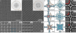
 Electron microscope images of radiation-sensitive 2D polymers, taken at the TEM with electron beams of reduced energy (120 keV) / (Image: Baokun Liang / Ulm University)Professor Kaiser describes 2D polymers as the 'young and wild' among polymers. This is because they react sensitively if you want to examine them more closely. The molecular interactions of organic 2D polymers are very complex and sensitive to interference due to the different types and properties of the bonds. Until now, it has hardly been possible to characterize such materials using electron microscopy with sufficient resolution at the atomic level. According to the physicist, the problem is that the imaging electrons interact with the atoms of the polymer layer and can damage or even destroy them.
In collaboration with researchers from Dresden, Halle and Leipzig as well as Guangzhou and Jinan (China), a research team from Kaiser's working group has succeeded for the first time in examining 2D polymers at almost atomic resolution on a TEM without damaging them or changing their composition. They used the TITAN microscope from Ulm University, a high-resolution and image error-corrected TEM.
For their investigations, the researchers varied the acceleration voltage and number of electrons in order to find out at which parameters the highest image quality can be achieved with minimal electron beam damage.
Electron beams with an energy of 300 keV are usually used for transmission electron microscopy imaging of organic materials. The physicists from Ulm, however, worked with low voltage and low electron doses for their study. The energy of the electrons was reduced from 300 to 80 keV. This showed that a voltage of 120 keV - with a simultaneous reduction in the number of electrons - produces the highest possible resolution in the image.
For their experiments, the scientists initially used 2D polymers with a crystalline structure. Their regular structure is easily recognizable under the microscope. This allowed electron beam-related defects to be easily detected as irregularities and pattern deviations. A new AI-based evaluation system also helped the scientists with this. After determining the optimum imaging conditions at the TEM for crystalline 2D polymers, the experiments were extended to amorphous polymers.
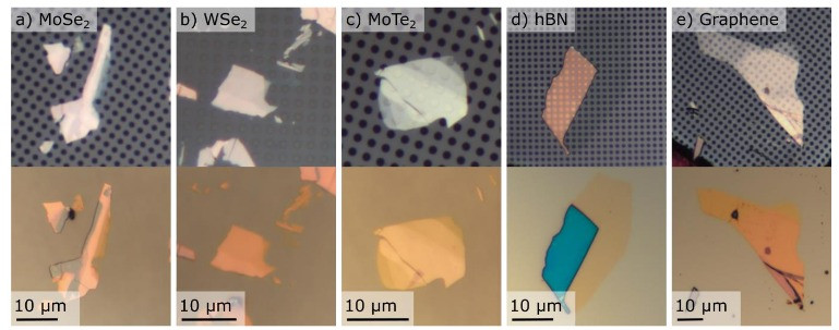
 Optical micrographs before and after reverse transfer of various 2D materials. Top: Electron beam exposed 2D material on a TEM grid before reverse transfer. Bottom: 2D material successfully reverse transferred onto a polystyrene substrate (a) MoSe2, (b) WSe2, (c) MoTe2, (d) hBN and (e) graphene
The results
According to Kaiser, the research group succeeded in significantly increasing the resolution at a lower acceleration voltage. For the first time, a high-contrast, detailed image of the structure of thin organic polymer layers was obtained at a near-atomic level. The work of the German-Chinese research team therefore makes it possible to identify molecular defects that have a decisive influence on the material properties and therefore on the potential applications. The 2D polymers for the study were synthesized at Sun Yat-sen University (Guangzhou/China) and TU Dresden. The calculations on the quantum mechanical properties of the defect structures were also carried out in Dresden.
The study was published in the journal 'Nature Communications'.
www.uni-ulm.de, www.tu-dresden.de, www.sysu.edu.cn/sysuen/


