As more and more high-performance processors are being installed in ever larger systems, for example in data centers, not only is the energy requirement growing, but also the amount of cooling media and technology required for cooling. Experts in many countries are looking for more efficient, cheaper and environmentally friendly cooling solutions to prevent microelectronics from reaching its limits.
On the one hand, the structures of integrated circuits are becoming smaller and smaller every year and also generate more heat per unit area. On the other hand, the dimensions of the chips are growing because more and more functional units are being integrated on one chip. There is also a trend towards 3D chip stacking. This applies in particular to microprocessors and memory. All in all, high-performance electronic devices and systems are consuming more and more electricity and generating more heat.
Experts from management consultants McKinsey estimate that data centers currently consume more than 1.5% of the electricity produced worldwide. According to market analysts' calculations, this figure will rise to 5% by 2030 due to the rapid growth of digitalization, particularly the triumph of artificial intelligence and cryptocurrencies.
Cooling limits soon to be reached
As AI workloads grow rapidly, the need for unprecedented computing power is pushing current cooling technologies to their limits. Conventional methods such as air, liquid and immersion cooling are effective over large areas, but are increasingly unable to cope with the extreme heat generated in the dense, power-laden areas deep inside processors. This limitation has already slowed progress in clock speeds and single-thread performance. Therefore, innovations in cooling technology are urgently needed to keep pace with semiconductor development. However, there are also increasing problems with the communities where the huge computer centers are located: The quantities of water required for traditional cooling can be provided less and less due to climate change, i.e. the scarcity of water that often accompanies it. Sustainability requirements for large consumers are rapidly coming to the fore. Energy-efficient, water-free cooling solutions are urgently needed to achieve environmental goals.
Intensive international search for solutions
In global research, different approaches are being taken to solve the problems. Some, for example, are continuing to concentrate on water cooling, but are modifying it. Others are trying to break completely new ground. The successes vary greatly. A few examples are presented below.
Intel is testing a new but classic water-based approach to cope with the increasing heat development of its chips. At Foundry Direct Connect (April 29, 2025, San Jose, USA), the company presented an experimental package-level water cooling solution to cool CPUs more efficiently(Fig. 1). Intel already has working prototypes for both LGA (Land Grid Array) and BGA (Ball Grid Array) CPUs, including demos with Intel's Core Ultra and Xeon server processors [1].
The cooling solution does not direct the coolant directly to the chip. Instead, a specially developed, compact cooling block sits on the chip housing. It has copper microchannels that precisely control the coolant flow. These channels can be optimized to target specific hotspots on the chip to improve heat dissipation where it matters most.
The company states that the system can dissipate up to 1000 watts of heat with standard liquid coolants. This type of heat load is atypical for consumer CPUs, but could be relevant for high-end AI (artificial intelligence) workloads, HPC (high performance computing) and workstation applications.
The cooling unit is also said to use solder or liquid metal TIM (Thermal Interface Material), which is said to provide better contact than polymer-based TIM. Compared to a conventional liquid cooler mounted on a bare die, Intel claims this solution provides 15-20% better thermal performance.
It is worth noting that Intel's approach is not just a laboratory experiment. The company has reportedly been working on this technology for years. In view of the increasing thermal requirements of modern chip designs, Intel is now researching how this system can be produced for practical use. However, in terms of performance, this solution is still a long way from the general improvement in cooling that other research institutes are striving for.
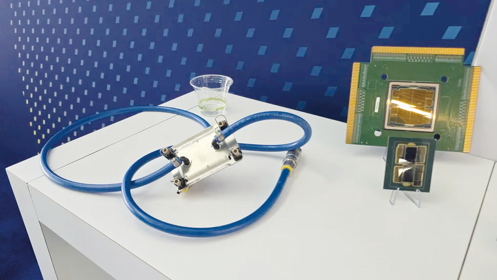 Fig. 1: Demo example of Intel's improved cooling solution
Paradox: Cooling with boiling water
For example, a research team from the Institute of Industrial Science at the University of Tokyo has developed a new cooling solution that uses the phase change of water to dissipate heat more efficiently [2]. According to SciTech Daily in April 2025, water absorbs seven times more energy when it changes phase from liquid to gas (i.e. boiling) and can therefore absorb and dissipate more heat than the conventional method using flowing water. However, as the coolant flows through tiny capillaries that are integrated directly into the chip, the vapor often has difficulty flowing through these narrow channels. This often makes the solution less efficient than conventional methods.
The researchers solved this problem using 3D microfluidic channels with a capillary structure and a distributor layer(Fig. 2). They discovered that the shape of the microchannels and the way the coolant is distributed in the system significantly affect its thermal and hydraulic performance. By ensuring a continuous flow of water and vapor, the team achieved a coefficient of performance (COP) of 100,000 - around ten times higher than with single-phase water cooling. This is significantly more than Intel's new solution.
"Thermal management of high-performance electronic devices is critical to the development of the next generation of technology, and our design potentially opens up new avenues for the required cooling," said senior author Masahiro Nomura. The use of this two-phase system could enable more compact cooling solutions without the need to develop or use more exotic fluids.
In addition, it could solve the thermal problems of high-performance computing and lead to more powerful chips with lower cooling power requirements. According to the Japanese researchers, this technology can also be used in other applications such as lasers, photodetectors, LEDs and radar systems, as well as in the automotive and aerospace industries. The system can also work passively, so that the changing phases of the liquid dissipate heat by convection and function without a pumping mechanism. Before moving on to the next cooling solution, this article will introduce another aspect associated with the search for suitable cooling solutions, namely the question of validating solutions.
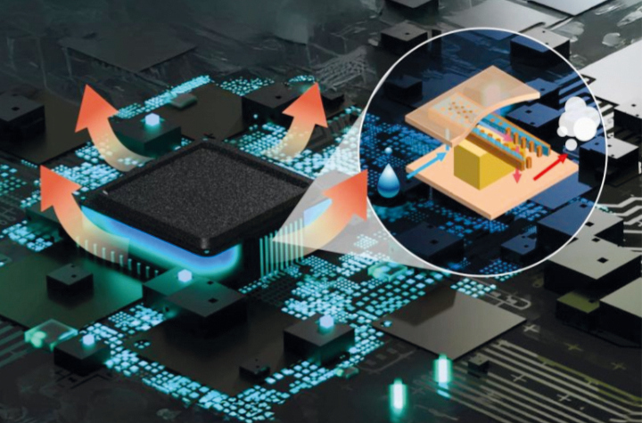 Fig. 2: Schematic diagram of the cooling solution at the University of Tokyo
3D stacks magnify the cooling problem
With the growing demand for more powerful and efficient microelectronic systems, the industry is turning to 3D integration, i.e. stacking chips on top of each other. This vertically layered architecture could allow high-performance processors, such as those used for artificial intelligence, to be tightly packaged with other highly specialized chips for communications or imaging. However, the transition to ICs with 3D stacked structures raises the cooling problem to a much more complicated level in the future than with ICs with a planar arrangement of cells. Technologists everywhere are faced with a major challenge: how can these stacks be prevented from overheating? It must therefore be clarified as early as the development phase of such 3D chips whether the envisaged cooling solutions are effective.
According to a press release from April 2025, the MIT Lincoln Laboratory (USA) has developed a specialized chip to test and validate cooling solutions for packaged chip stacks [3]. The chip fulfills two functions: heat generation and temperature detection. It dissipates extremely high power and mimics high-performance logic chips that generate heat through the silicon layer and in localized hotspots. When cooling technologies are then applied to or in the packaged stacks, the chip measures the temperature changes. When embedded in a stack, it can allow researchers to study how heat moves through the stack layers and better compare the benefits of different possible cooling solutions(Fig. 3).
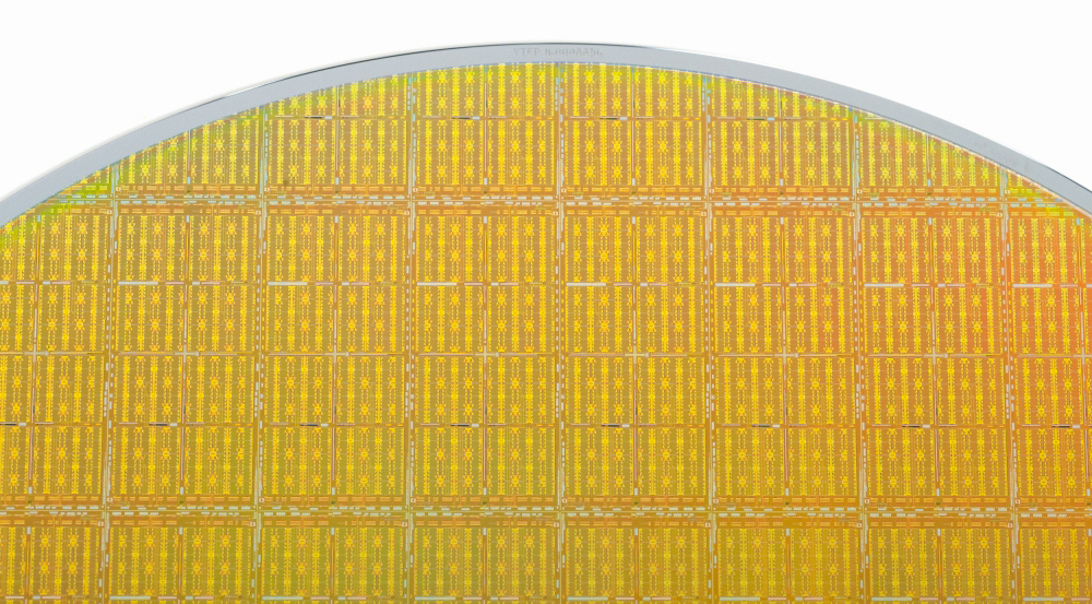 Fig. 3: This silicon wafer contains chips for testing cooling systems for three-dimensional integrated microelectronics. Each chip consists of circuits that generate heat within a 3D stack and measure the temperature when cooling solutions are inserted or applied
"If you only have a single chip, you can cool it from above or below. But if you start stacking multiple chips on top of each other, there's nowhere for the heat to escape. Today, there are no cooling methods that allow the industry to stack multiple of these really powerful chips," said Chenson Chen, head of the Laboratory's Advanced Materials and Microsystems Group at MIT. The benchmarking chip is now being used at HRL Laboratories, a research and development company jointly owned by Boeing and General Motors, in the development of cooling systems for 3D heterogeneous integrated (3DHI) systems. Heterogeneous integration refers to the stacking of silicon chips with non-silicon chips, such as III-V semiconductors used in radio frequency (RF) systems. RF components can get very hot and run at very high powers - this adds an extra layer of complexity to 3D integration, which is why this test function is so important. The benchmarking chip developed can operate at very high power densities in the kilowatt/cm range, comparable to the predicted power requirements of high performance chips today and in the future. More detailed information is given in [3]. In terms of performance, it therefore corresponds to the Minitherms3D project cited below. The Defense Advanced Research Projects Agency (DARPA) of the US Department of Defense funded the development of the benchmarking chip by the MIT lab in support of the HRL program. All of this research comes from the DARPA program 'Minitherms3D' (Miniature Integrated Thermal Management Systems for 3D Heterogeneous Integration). This shows how serious the US military-industrial complex is about solving cooling problems. The DARPA project, which has been running since 2023, aims to reduce the overall thermal resistance by more than 3 times and increase the volumetric thermal management capability by a factor of two [4]. Figure 4 demonstrates the tasks to be solved.
Interested parties can find a detailed project description in the 57-page DARPA document 'Miniature Integrated Thermal Management Systems for 3D Heterogeneous Integration (Minitherms3D)' from the Microsystems Technology Office of the institution [5].
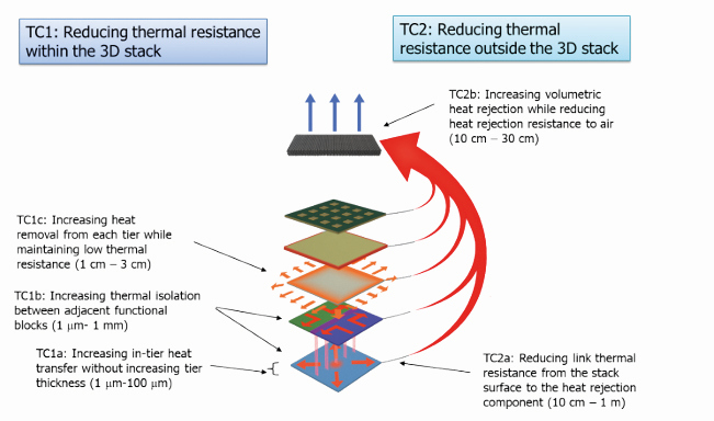 Fig. 4: Challenges in the area of multi-scale thermal management inside and outside a 3DHI stack according to the DARPA project
Laser use for server cooling - MXL Laser Cooling
The US start-up Maxwell Labs (commonly known as MXL Labs) wants to take a more rigorous step towards cooling high-performance components than other universities and companies. In a press release from April 2025, it was explained that researchers from Sandia National Laboratories, together with colleagues from Maxwell Labs and the University of New Mexico (UNM), want to use laser cooling to reduce the energy consumption of data centers on the basis of a CRADA (Cooperative Research and Development Agreement). Instead of using water or air, the microprocessors in the countless servers are to be cooled with laser beams in future. As this process is more effective, the computing power can be increased despite the lower power consumption. This is because cool chips calculate faster than hot ones [6].
Under the CRADA, Maxwell Labs will provide the technical designs, Sandia Labs will use its expertise in molecular beam epitaxy to fabricate high-purity gallium arsenide (GaAs)-based components, and UNM will evaluate the thermal performance of the resulting systems. Sandia's decades of experience in manufacturing high-quality semiconductors - supported by its role in the Center for Integrated Nanotechnologies (CINT), a DOE Office of Science user facility - ensures the precision and purity required for the photonic cooling system's success. The cooling of gases by laser can be explained relatively clearly. The beam acts against the movement of the hot molecules and slows them down. This is comparable to a rolling billiard ball colliding with a ball moving in the opposite direction. If both speeds match, they remain stationary after the collision.
Photonic cold plate
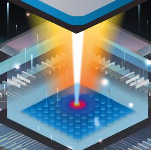 Fig. 5: Schematic representation of highly effective laser cooling. CPU and GPU processors have a higher power density than the core of a nuclear reactor - photonic cooling targets these areas with lasersTheprinciple also works with solids, using a photonic cooling plate that is made of the semiconductor material gallium arsenide and is less than one millimeter thick. A fine laser beam with a very specific frequency is fired at this plate. It slows down the molecular movements. The plate cools down. The researchers want to use this to remove heat from microprocessors and other semiconductor components.
As laser light heats up impurities and would therefore nullify the cooling effect, the cooling plate must consist of extremely pure, thin gallium arsenide layers. This is achieved by molecular beam epitaxy, in which the layers are deposited molecule by molecule on a substrate.
Maxwell Labs is located in Saint Paul (Minnesota). It is led by a young team of industrial and academic leaders who are highly skilled in supercomputing, nanoscale heat transport and photonic engineering, some of whom have emerged from leading universities in the USA. The goal is for MXL Labs to pioneer the next generation of high-performance computing with its patented laser cooling technology. By converting heat into light, MXL's innovative approach bypasses several limitations of traditional cooling methods to solve one of the most critical challenges in AI and HPC (High Power Computing) - thermal management.
Three key points
The company's goals can be outlined in six key points:
- Hotspot targeting: thermal management that targets chip hotspots and improves cooling efficiency directly at the source
- Performance enhancement: enabling chips to operate at higher speeds without thermal throttling
- Increased energy efficiency: the by-product of the technology is light that can be recycled and efficiently returns power to the data center
- Increased reliability: No moving parts or working fluids, resulting in increased reliability, reduced maintenance and ease of operation
- No working fluids: Eliminating the use of fluids, reducing the risk of leaks, simplifying maintenance, promoting water conservation
- Scalability: scalability with future chip design and power supply requirements without the need for extensive design changes
From Figure 6, which shows the basic function of the system called MXL Photonic Coldplate, it can be seen that it is a closed-loop system with additional partial energy recovery.
 Fig. 6: Function of the MXL Photonic Coldplate System
Objectives, sponsors, processes
"MXL Labs is developing a prototype for laser cooling that is designed to achieve a 200% increase in performance on the latest NVIDIA or AMD hardware with a 40-fold increase in efficiency compared to liquid cooling
with the same net performance," says Managing Director Jacob Balma.
The project is highly regarded by experts:
- Henry Newman, former CTO of Seagate Government Solutions: "This technology enables new chip designs that allow unprecedented performance gains in processors"
- Earl Dodd, World Wide Technology, global market leader for HPC and emerging technologies: "Groundbreaking technology. Opens up incredible possibilities for effective power supply and cooling"
The circle of sponsors is correspondingly large. It includes academic institutions (Massachusetts Institute of Technology, Princeton University), government institutions (Department of Defense, U.S. Air Force, ML Performance, DEVCOM Army Research Laboratory), companies (AMD, Hewlett Packard, CRAY) and the government-owned Sandia National Laboratories mentioned at the beginning. The importance of the project for the US military-industrial complex can hardly be emphasized more.
MXL Labs has a 3-phase Early Access Program (EAP), in which selected strategic customers are acquired for pre-licensing opportunities. The individual phases are as follows:
- EAP 01: Pre-license pilot phase, December 2024
- EAP 02: Evaluation demo phase, July 2025
- EAP 03: Integration pre-order phase, January 2026
The EAP offers exclusive, limited access to MXL-Gen1 photonic cooling technology for selected data centers, chip manufacturers and system integrators. EAP participants will gain early insights through pre-release performance data, hands-on design optimization opportunities, and a first-mover advantage in testing on real hardware and server integration.
MXL Labs is already making a big splash. However, apart from such promotional presentations of principles as in Figure 7, there are still no official details about the exact technical realization of the photonic coldplate system, although the first evaluations with current hardware are to be carried out with EAP 02 in July 2025. On the excellently designed MXL website, numerous examples of the future practical benefits of the new cooling method are demonstrated both in the social sector and in the military and defense industry [7].
 Fig. 7: Effective advertising principle illustration of the Photonic Coldplate System
Sandia's role as a major research institution in the project
Sandia National Laboratories was mentioned at the beginning as the main partner of MXL Labs. This should make it clear that the main focus of the project is likely to be on the military and defense industry sector. Sandia (SNL for short) is a research and development facility of the US Department of Energy founded in 1948 with sites in Albuquerque, New Mexico, and Livermore, California, and around 12,000 employees. Its main task is to develop, manufacture and test the non-nuclear components of nuclear weapons. In addition, SNL developed suborbital research rockets such as the Strypi and STARS, which are used for system testing of ballistic weapons and missile defense systems [8].
Sandia has been operating the Red Storm supercomputer from Cray Inc, also a sponsor of the MXL project, since 2004. The system consists of 14,348 computing nodes, each consisting of a dual-core AMD Opteron processor for computing tasks and a PowerPC 440-based processor (SeaStar) for communication tasks. It is therefore not surprising that MXL chose AMD hardware as its first test bed to help Cray and Sandia develop a future-proof, more efficient successor to Red Storm [8].
Patents
To conclude this report, let's take a quick look at the patents as a crucial intellectual basis for the project. MXL Labs bases its project on several of its own patents, some of which were only disclosed in April 2025, when the press release on the project was issued. Patent no. 11435766 (filing date 9/9/2019) and patent no. 2287651 (filing date 22/7/2022) have the same title: Fine-grain dynamic solid-state cooling system. They set out the basic operating principle of the cooling system in detail [9, 10].
MXL Labs believes that the successful realization of the project will have a decisive impact on the entire electronics development chain, from circuit development and design to the operation of finished devices and systems. It will be in the hands of electronics developers to implement the new possibilities of cooling.
References
[1] www.techpowerup.com/336164/intel-prepares-1-000-w-package-attached-liquid-cooling-modules (Retrieved: 18.6.25).
[2] www.iis.u-tokyo.ac.jp/en/news/4747/ (Retrieved: 18.6.25).
[3] www.ll.mit.edu/news/new-chip-tests-cooling-solutions-stacked-microelectronics (Retrieved: 18.6.25).
[4] www.darpa.mil/research/programs/Minitherms3D (Retrieved: 18.6.25).
[5] fundingforecaster.net/lansync/wp-content/uploads/2023/02/HR001123S0019-1.pdf (Retrieved: 18.6.25).
[6] mxllabs.com/ (Retrieved: 18.6.25).
[7] mxllabs.com/industry-solutions/ (Retrieved: 18.6.25).
[8] en.wikipedia.org/wiki/Sandia_National_Laboratories (Retrieved: 18.6.25).
[9] patents.justia.com/patent/12287651 (Retrieved: 18.6.25).
[10] patents.justia.com/patent/11435766 (Retrieved: 18.6.25).


