
Increasing wiring density on the PCB surface is becoming a challenge for CAD design and PCB production. More complex contacting strategies, reduced via, pad and track areas and more complex multilayer design are possible solutions.
The evolution of electromechanical assemblies is obvious: the density of connections on the components is increasing. This becomes most obvious when looking at the pin spacing (~ pitch) of BGAs. The usual value is still 800 µm, but the trend is towards 650 µm. The evolution of components has not yet ended with BGAs with a pitch of 500 µm. The limit is BGAs with a pitch of 400 µm, which are already used in hundreds of thousands of cell phones.
The placement density of components on the surface of a PCB is also increasing. Double-sided placement is common and if the available space on two sides is no longer sufficient, placement on the third or fourth level is considered: The 'embedded components' principle is leaving the test phase behind and will soon be a challenging but common option.
Looking ahead
The routing of the resulting extremely high wiring density on the PCB surface will become a massive challenge for CAD design and even more so for the production of the required PCB. The solution can only lie in a more complex contacting strategy, in reduced via, pad and track areas and in a more complex design of the multilayer.
The current limits in the existing regulations are beginning to falter. Minimum trace widths and spacings of 100 µm, minimum drill diameters of 100 µm and the usual 25 µm copper thickness in the via sleeves can no longer fulfill the tasks at hand. The focus is therefore shifting to PCB technology.
The wiring density leads to the unavoidable situation that electrical signals have to be routed over several layers. This is only possible
- if a dynamic and flexible contacting strategy can be implemented
- if the previous geometric limits are undercut
- if the number of layers per multilayer increases and
- if the increasingly important physical specifications are still adhered to.
The logistical and economic framework conditions cannot remain the same. Printed circuit board manufacturers must increase their investments in system technology for the production of printed circuit boards. Another key position is occupied by employees, without whose expertise even the best systems are useless. Printed circuit boards are becoming more expensive. But that has to be the case and is a good thing, because without regular investment, the coming product diversity will significantly weaken Europe's position in international competition.
Partnership-based cooperation in the three disciplines of CAD design, PCB technology and component production must become more intensive. Increasingly, the fourth discipline is testing, because strategic decisions in the areas of IoT, smart home, cloud computing, IT security, Industry 4.0, G5 and big data demand reliability at a high level.
Multilayer construction plans
Detailed pictorial documentation of the layer structure is mandatory for communication between customer and supplier. Rudimentary black and white graphics and simplified Excel charts are useless and are a thing of the past.
Today, at least the base material, the distribution of prepregs, laminates and copper thicknesses, the contacting strategy, the file allocation and the physical requirements must be clearly defined and recognizable.
The time for the construction of the multilayer construction plan shifts towards the creation of the circuit diagram, as the information is important from the very beginning of a project. In addition to the technical description of an individual layer structure, the construction plan takes on a legal quality and is part of the customer's order and the PCB manufacturer's order confirmation.
There are currently three basic construction variants for rigid multilayers: the classic standard, the any layer and the dual core.
1. standard
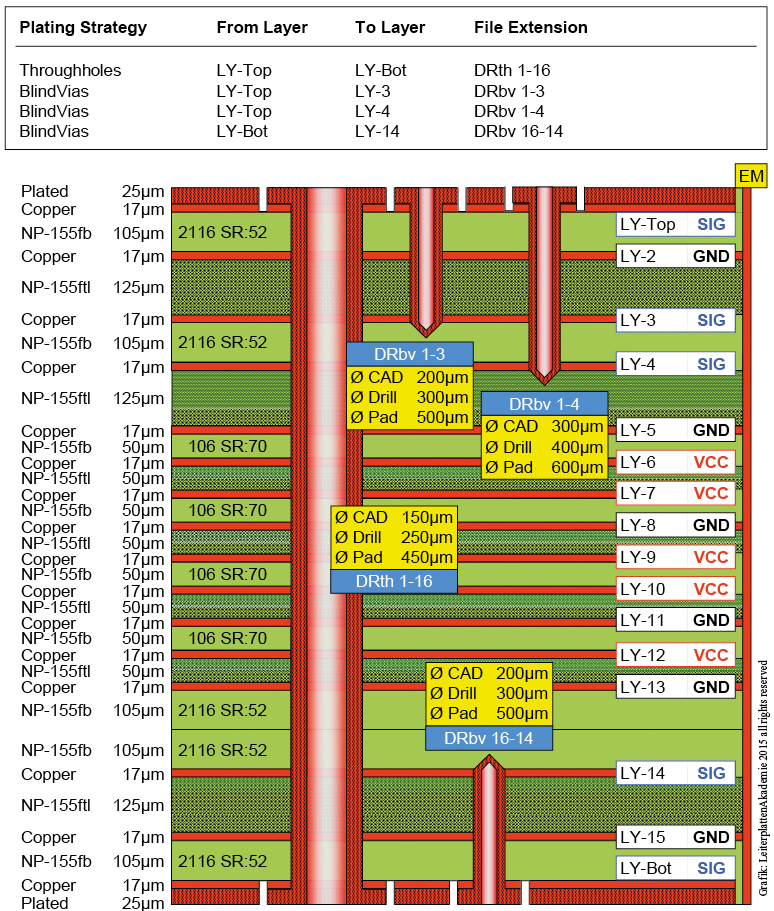 Standard layer structure
The contacting option must be defined in the constraints in the CAD system before routing begins. This not only defines the specifications for the physical function of the assembly, but also the layout strategy and the costs for the PCB. If the requirements change during the CAD design - especially if the number of layers is increased and/or the contacting strategy is changed - the layer concept must be rethought.
A single bonding/pressing of the base materials is provided for standard designs. In the first stage, only through-hole plating is planned for the connection between the layers. In the second stage, an addition with drilled and/or lasered blind vias starting from the top and/or bottom layer is accepted.
In principle, the three-dimensional structure of a layer stack-up should be divided into spaces for signal transfer and power supply. The number of signal layers depends on the number of nets to be wired, the pin spacing (~ pitch) of the most complex component and the required power layers. BGAs are typical and decisive.
The function and the application area of the module determine at the time of project planning which layer structure must be provided for the solution of the tasks.
For an FPGA with a fully occupied matrix of 25 x 25 columns and rows, a maximum of 5 signal layers are required for routing. There are 6 layers for GND and a total of 5 layers for VCC. The GNDs are distributed in such a way that impedances and return currents are defined.
The combination of 6 GND-VCC pairs with 50 µm spacing provides internal capacitance in the multilayer for an effective power supply.
The costs for a layer structure depend on the number of layers, the contacting strategy and the PCB class, i.e. ultimately the number of production steps to be carried out during the manufacture of the PCB. Approximately 48 steps are required to manufacture this PCB. There is only one pressing. The temperature load on the base material is low. The geometries are within the usual range.
With good and well-maintained production facilities, this multilayer can be purchased internationally from many PCB manufacturers. The functional reliability is high in the long term.
Design restriction with clearances
However, there is a limitation with regard to the free space for routing the CAD design. Vias are unfortunately indispensable, but reduce the paths for routing the signal traces.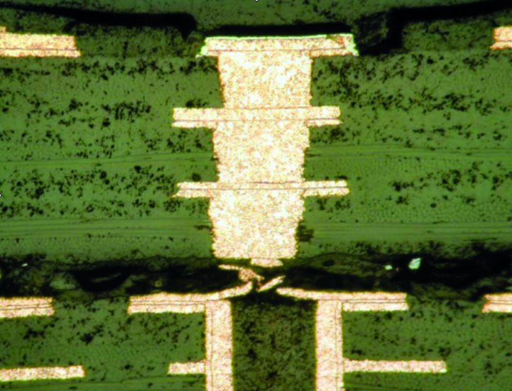 Adherent delamination with an 'any layer' structure
A via specified in CAD with a final diameter of 100 µm is usually drilled with a drilling tool diameter of 200 µm. With an aspect ratio (for contacting) of 1:8, the multilayer can then be a maximum of 1.60 mm thick. A Viapad diameter - plus safety clearance - is 600 µm, a track width and a track spacing of 100 µm.
In professional routing, the signal connection between two network points is only routed on two layers. The continuous via then blocks the path for 3 traces on the unused layers. If the number of signal layers increases due to the wiring density, the blockage for signal connections to be routed increases at the same time. This makes it difficult to adhere to the basic rule of routing traces directly from network point to network point over the shortest possible distance in order to keep the signal propagation time low and to optimize secondary conditions such as EMC and crosstalk.
2. any layer
A layer structure of the 'Any Layer' type has no continuous vias. The contacting strategy is to coordinate buried vias with stacked blind vias. If the length of the buried vias is over 300 µm, then filling of the buried vias by the resin potential from the prepregs becomes critical. Because the inclusion of air in buried vias is not permitted, plugging must be carried out.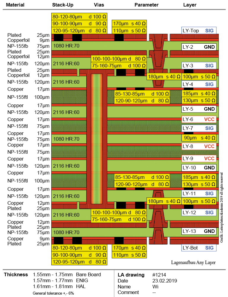 Layer structureAny layer
The internal blind vias must not be filled with epoxy resin and plugging with an electrically non-conductive substrate is also not permitted. Copper filling is the only option to ensure signal transfer via the blind vias on top of each other.
Contacting the blind vias and, if necessary, copper filling increases the copper thickness on the start layer of a blind via. The classic foil copper thickness of 17 µm and the classic copper contact thickness of 25 µm result in a total copper thickness of 42 µm. Etching narrow conductor tracks with a width of 100 µm becomes critical with this copper thickness. There is only a solution if the thickness of the foil copper is reduced to 12 µm, if not 9 µm, and/or if the thickness of the copper contact is reduced to 20 µm, if not 15 µm.
The physical requirement to place GND planes in the immediate vicinity of SIG planes to ensure return current paths and impedance references increases the number of layers to be superimposed and connected with blind vias.
Because blind vias have a short length and because each blind via usually only connects two layers, the inner layers have the necessary free space for routing high-density connections.
The priority of this layer structure is therefore to find a solution for the CAD layout. But design rules and reliability aspects shift.
It is not permissible to place blind vias on buried vias during routing. The analysis of errors on layouts previously routed in this way shows that the expansion coefficients of the plugging substrate of the buried vias and the surrounding base material often do not harmonize. The contact between the surface of a buried via and the underside of a blind via is not reliably stable due to the thermal stresses during the production of the PCB and the assembly as well as during assembly operation. Interruptions in the signal path lead to typical malfunctions and failure of the module.
A comparable, albeit somewhat lower, risk applies to blind vias stacked on top of each other. The hole created by the laser ablation must be absolutely clean and free of epoxy precipitation on the target plane so that the contact between stacked vias is reliable.
This requires individualized adjustment of the routing constraints on the CAD system. Avoiding the placement of a blind via on a buried via is not yet possible on every CAD system by default and is then dependent on the prudence of the layout designer.
Approximately 105 work steps are required to produce this multilayer. There are three pressings, which lead to a high thermal load on the base material. Because the aspect ratio (for contacting) for blind vias is only around 1:1, the distance between the adjacent pressed layers cannot be large. The usual differential impedances of 80 Ohm (... DDR3, DDR4) or 100 Ohm (... FPGA) can then only be realized with track widths and track spacings of up to a maximum of 75 µm. The advantage of the contacting strategy is offset by the disadvantage of the etching result.
At the latest after three pressings, such a structure becomes risky. Each pressing has an influence on the mechanical stability of the layer structure and the chemical consistency of the dielectric.
A few years ago, UL initiated a discussion on the 'solder limits' of a base material in order to get a grip on the thermal load capacity. This has justifiably shifted the focus from the Tg value to the Td value.
However, the soldering process at around 275 °C for a few seconds is not the only thermal load that the base material has to withstand. The pressing of a multilayer takes place at around 200 to 220 °C over a period of 90 to 120 minutes, i.e. three times for this layer structure.
If the long-term reliable function of an assembly is to be reliably assessed, then the pressing cycles and the soldering cycles must be considered and evaluated together. The author's personal rule is that a maximum total of 5 temperature cycles are permissible for the production of the PCB and the assembly of the module.
A multilayer of the 'any layer' type can currently only be purchased from a few PCB manufacturers nationally and internationally. The products are expensive and the functional reliability is risky.
3. dual core
The 'any layer' strategy of increasing the number of pressings and concentrating contacting on blind vias is already reaching its limits due to the arguments mentioned above. More promising is the construction of a multilayer consisting of (initially) two cores, the so-called 'dual core'. This construction of separate partial multilayers, which are later pressed into a complete multilayer, is simpler and more reliable.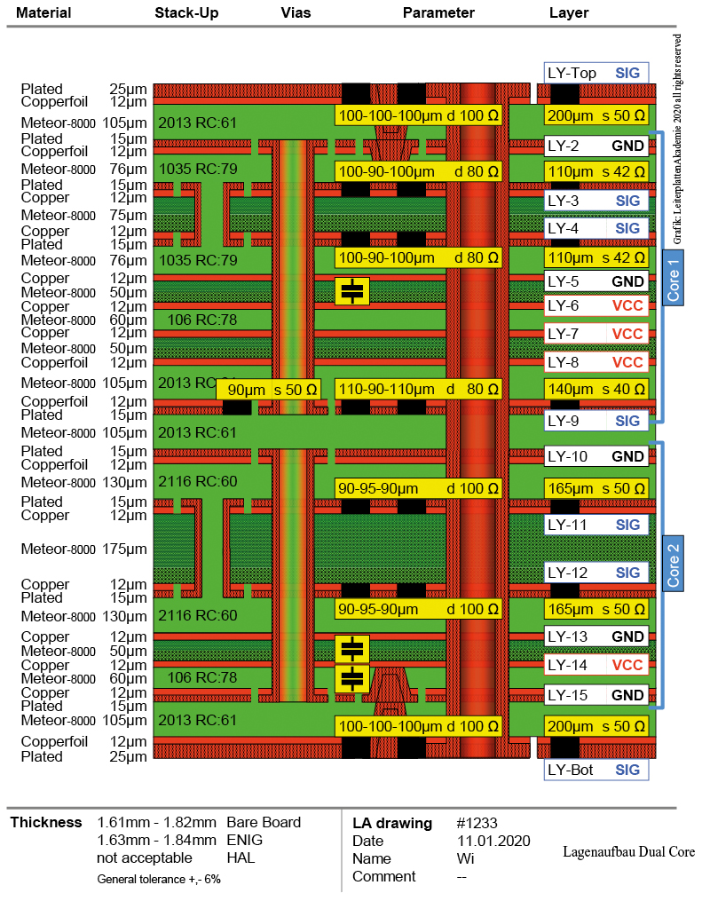 Dual core layer structure
The contacting strategy can be complex even for a maximum of two pressings of the PCB. The conductor track widths for compliance with the usual impedance values are ≥ 90 µm, which eliminates the etching process as a risky production step. The separate cores are mechanically stable enough and allow the upcoming requirement of 'embedded components', i.e. the assembly of the PCB on a third or even fourth level.
The priority of this layer structure is to find a stable solution for the assembly and the physical function. The 'dual core' structure has defined power planes and signal layers. The GND layers provide an optimized return current path, ensure high signal integrity and allow the usual impedance values.
In combination with the edge metallization in the layer structure, the GND planes create spaces with Faraday quality that can exclude crosstalk and offer optimum EMC behaviour for the module.
The power supply is located on 50 µm planes and 50 µm prepregs and acts as a multipower system for an effective power supply to the components. Additional capacitor groups (according to the Dirk principle) attenuate the resonance frequencies.
Approximately 79 work steps are required to manufacture the 'Dual Core'. There are 2 pressings. The temperature load for the base material is medium. The geometries are within the usual range. This multilayer can be purchased internationally from a number of PCB manufacturers. The costs are in the medium range and the functional reliability is high.
Summary
The technical-physical function of a multilayer must be reliably guaranteed. The documentation of a layer structure must show the base material in detail. The layer stack-up must ensure binding communication between CAD, PCB and assembly. The layer structure must have been agreed with the PCB manufacturer at the latest before the start of the CAD design.
