The Japanese EDA software manufacturer Zuken and the British research institute Compound Semiconductor Applications (CSA) Catapult have developed optimized tools for creating 3D models of power modules in a joint project. The aim of the research and development cooperation was to provide a development environment for modern compound semiconductor products.
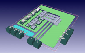
 Fig. 2: Example of the 3D design of a power module using CR-8000 Design Force's ability to capture ribbon bond wires and high current metal terminalsCSACatapult is a UK government-funded not-for-profit organization based in South Wales, established to help the UK become a world leader in semiconductor interconnect technology. CSA Catapult works with both large companies and start-ups to develop and commercialize new applications of semiconductor technology. The organization focuses on three technology areas:
- Power Electronics
- Radio frequency and microwave technology
- photonics
In addition to these three technology areas, CSA Catapult also works in the area of advanced packaging for the field of high-current technology. The joint work of Zuken Germany and CSA Catapult took place in the latter area. [1] While Zuken, as a leading provider of EDA software solutions for electronics design, contributed its chip, package and PCB co-design software CR-8000 Design Force, CSA provided its technological experience in the design of complex power modules, in particular modern compound semiconductor products.
Design for highly integrated semiconductor products
The collaboration between Zuken and CSA Catapult involved a project to transform the concept of a power module from a graphical sketch into a production-ready 3D model. A series of requirements and enhancements for efficient co-design of mechanical and electrical design for power electronics components were identified and implemented by Zuken as part of CR-8000 Design Force. In combination with integrated industry standard simulation tools, a development environment was provided that enables the design framework for new highly integrated semiconductor products to be efficiently explored in an iterative process.
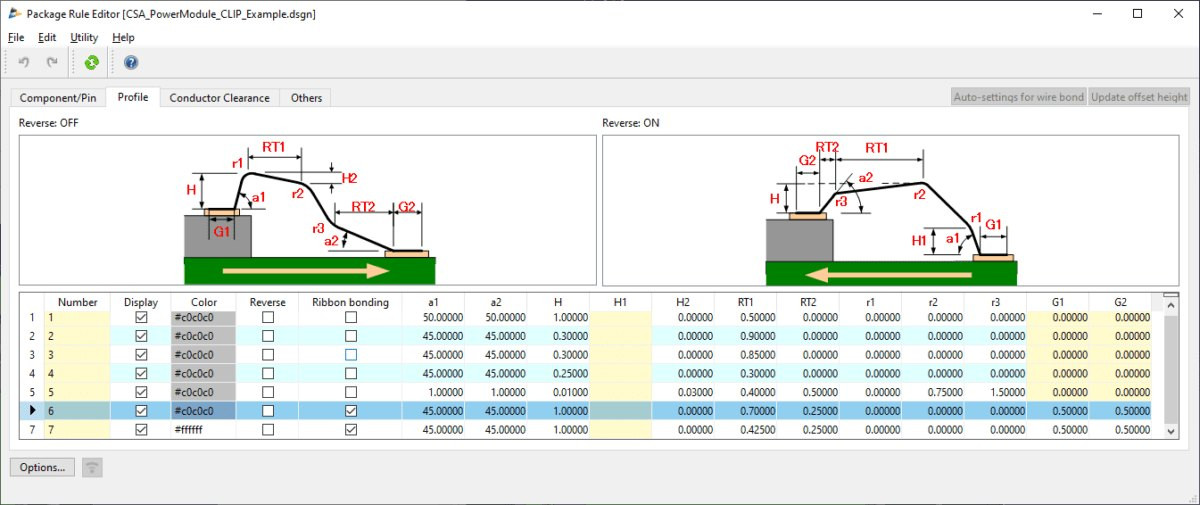
The result of the collaboration is an intuitive functionality for creating the interconnect structures between chips and copper layers on a substrate or PCB, as well as an export function for a CAD model in a format compatible with FEM software(Fig. 2, 3). These advanced features help designers to significantly reduce the time required to create a 3D model of the substrate, chip layout and chip-to-chip and chip-to-copper connections of a power module.
 Fig. 3: Package rule editor for clip design in power modules
Commenting on the progress of the research and development collaboration, Dr. Alejandro Villarruel Parra, Senior Power Electronics Engineer at CSA Catapult, said: "Creating a 3D model of the substrate, chip layout and chip interconnects is an important part of the early stage of the power module design process. Zuken's advanced design solutions have helped to preview the performance of the module and this speeds up our decision-making process when comparing multiple design concepts. After settling on an implementation concept, they provide valuable guidance for fine-tuning the geometric structures of the module."
The new feature is included in the 2022 release of CR-8000 Design Force.
Advanced Packaging Design Studio
Zuken's partner on the CSA Catapult side was the Advanced Packaging Design Studio. This was established to address the assembly and packaging challenges in the development of compound semiconductor modules and systems. Its task can be briefly outlined as follows:
- Develop innovative packaging solutions through packaging design and modeling, micro-assembly and rapid prototyping
- Enabling the development of next-level integration technologies that combine design and advanced interconnects
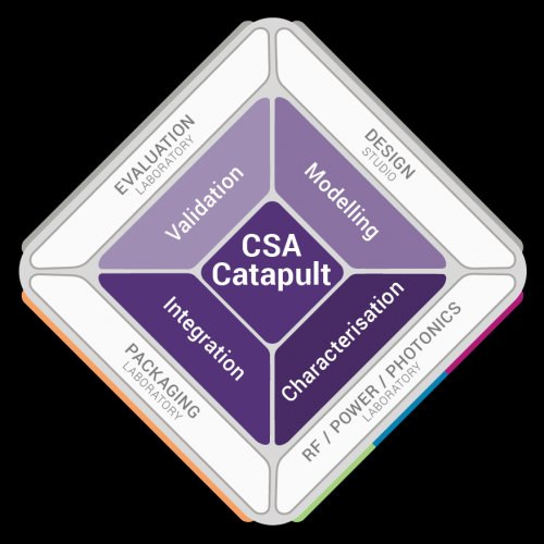
The functions of the studio within the research facility are symbolically illustrated in Figure 4.
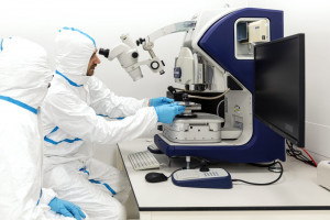
An ISO Class 7 clean room provides the optimal environment for low-volume semiconductor assembly processes, product development and scale-up services(Fig. 5). The advanced packaging engineers are currently focusing on packaging solutions for power electronics, RF modules and photonics. The engineers' expertise is designed to turn customer ideas into proof of concepts/prototypes and help bring them to market effectively and quickly. Webinars are used to pass on the knowledge gained to the industry in a targeted manner.
The studio's modeling equipment includes the following tools:
- Comsol and Ansys
- Solidworks
- Zuken CR-8000
The task of Comsol and Ansys is the multi-physical simulation of housing modules using integrated mechanical, electrical, photonic and thermal test scenarios in order to obtain correct prototypes the first time.
Solidworks is used for 3D capture of the mechanical design of packaging components and assemblies. It is integrated with multiphysics software for an efficient design simulation process.
The task of CR-8000 is chip-package-board co-design for power, photonics and RF. The EDA tool works in context with the other two tools mentioned.
EDA tool CR-8000
 Fig. 5: The clean room is equipped with state-of-the-art technologyCR-8000is a comprehensive PCB design software system that supports the development of electronic assemblies from concept to production. CR-8000's end-to-end integrated design flow extends from initial system planning, where basic decisions are made about partitioning, component selection, form, fit and function of the product or system, through the creation of detailed schematics and layout of single and multi-board PCB systems, to manufacturing optimization. A modular, object-oriented architecture ensures consistency of all data and versions from concept to production.
It is the only PCB design software that is complemented by a data management functionality that enables comprehensive library, module, configuration and release management.
Equipment configuration
In order to gain a more detailed insight into the technical working possibilities of the Packaging Design Studio, we will also take a look at the laboratory hardware. The technical equipment includes
- Form 3 3D printer for printing polymers
- Hesse BJ653 Manual/Semi-Automatic multi-purpose wire bonder
- Tresky T-3003-Pro + high pressure sintering attachment
- Nordson-Dage Prospector Universal Micromaterial Test System
The Hessian bonding system provides manual and automated wire/tape bonding for wire thicknesses from 12.5 µm gold or aluminum to 600 µm aluminum wire and up to 2 mm wide tape bonding to meet a variety of RF, photonics and power packaging requirements.
The Tresky equipment enables manual die attach/die bonding for experimentation and low volume prototyping. It allows high/low pressure sintering, eutectic, ultrasonic bonding as well as epoxy die attach. It also supports flip-chip and clip bonding with highly accurate alignment capability down to +/- 1 micron.
The Nordson system enables advanced bonding and material testing, shear testing up to 200 kg, tensile testing up to 100 kg and compression testing up to 50 kg. It also performs high-precision visual inspections, load (bend) tests, scratch tests, bend and twist, creep and thermal stress tests for complete assembly characterization.
Please refer to the introductory image of the article(Fig. 1), which demonstrates the possibilities of the studio and can be realized with the help of CR-8000.
www.csa.catapult.org.uk, www.zuken.com/de/


