
The increasingly revolutionary developments in the fields of mobility or IoT and the acceleration of digital change driven by coronavirus require a significant increase in research intensity in the microelectronics industry. In technological terms, this means not only maximum reliability and maximum power and functional density, but also increasing component functionality, which can be achieved through finer structures, heterogeneous system integration in the form of system-in-package (SiP) or system-on-chip (SoC) and, above all, the use of the 3rd dimension in packaging. "A new era for 3D has dawned," said E. Jan Vardaman from TechSearch International in Texas at the 3D & Systems Summit 2020 in Dresden in January. Saxony's microelectronics elite is focusing on More than Moore and three-dimensional chip structures, specialties of Saxony's companies and researchers.
Germany can digitization and technology
Connectivity+computing+cloud is the core driver of the smart society. "The explosive growth of data-generated and global network traffic is changing the structure of the economy," emphasized Laith Altimime, President of SEMI Europe in January. Uwe Peter, Head of Germany at Cisco, summarized in May: "In recent weeks, we have seen what a digital Germany can look like. When it comes down to it, Germany can digitize at the speed of light. We have used technology to maintain our coexistence, our economy and our administrative, government, education and healthcare systems. And we have realized that it works. This should encourage us to continue along the path of digitalization with even more determination." 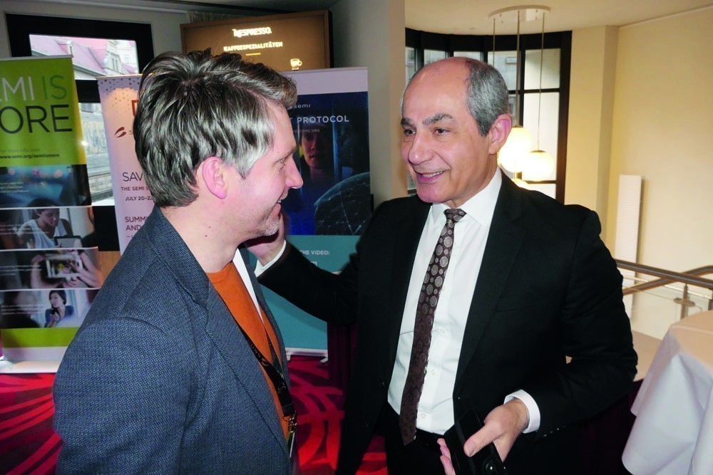 The President of SEMI Europe, Laith Altimime, in conversation with Michael Kaiser/Smart Systems Hub Dresden GmbH (left )
On the one hand, market demand is increasing for faster and specialized logic chips that make voice-controlled digital assistants or artificially intelligent systems possible in the first place. On the other hand, many new mobile devices are in demand for universal all-in-one chips, data transmitters, processors and sensor phalanxes that consume very little power and cost very little. In the past, the focus was simply on chips with smaller structures (More Moore). Now the industry has to adapt to a fundamentally higher functional density of products (More than Moore) and invest significantly more in R and D. There are more and more physical limits to overcome and suitable factories cost tens of billions. The coronavirus crisis has only slowed the industry down slightly: although sales at MEMS contract manufacturer X-Fab Silicon Foundries from Erfurt/Dresden fell by 3% in the first quarter, the order volume increased by a quarter, announced CEO Rudi De Winter. In May, the company started up a new line for SiC power semiconductors.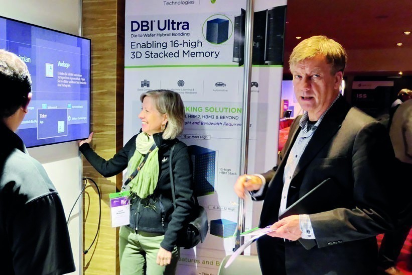 Laura Mirkarimi, here at the Xperi Co. information stand, gave a presentation on the Xperi-DBI ultra die-to-wafer hybrid bond technology (16-fold 3D stacked memory), on the right M. Jürgen Wolf (Fraunhofer-IZM/member of the SEMI organizing committee).
Microelectronics experts met in Dresden
The Saxon state capital of Dresden once again hosted the 'SEMI 3D & Systems Summit' in January. Top representatives from the world's leading industry players Intel, TSMC, Infineon, ASML, Globalfoundries, Huawei, IMEC and CEA-Leti were among the more than 300 participants at the annual meeting of the global microelectronics association SEMI, which has been held since 2009. The background to this year's 3D summit was this rethinking process in the industry: due to immensely rising costs and technological challenges, "business as usual" is no longer possible for the semiconductor industry. It is thanks to the strong microelectronics/ICT cluster - every second chip manufactured in Europe comes from Dresden - and the distinctive expertise in 3D and heterogeneous system integration that this top-class meeting has been held in Dresden again for the last three years with steadily growing interest.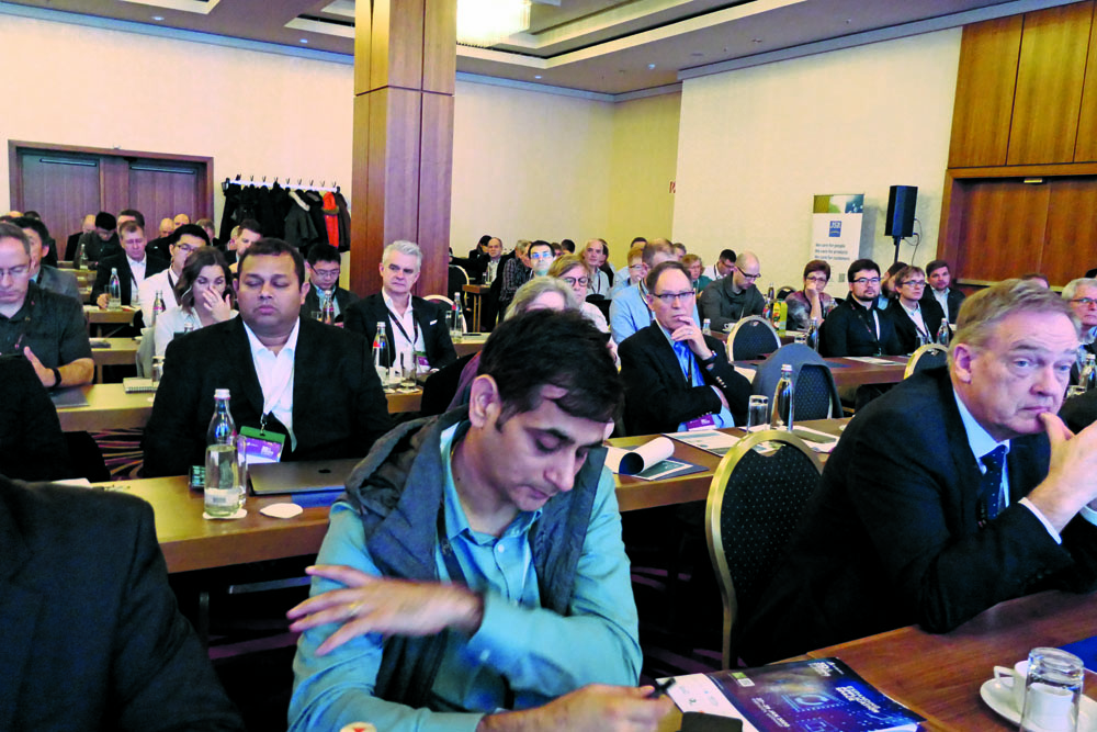
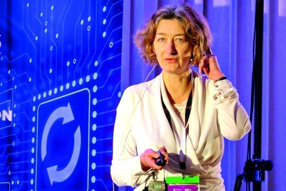 In the 'Grand Ballroom' of the Hilton Hotel in Dresden, Séverine Cheramy from the French research center CEA-Leti spoke about the wave of innovation in 3D VLSI technologies
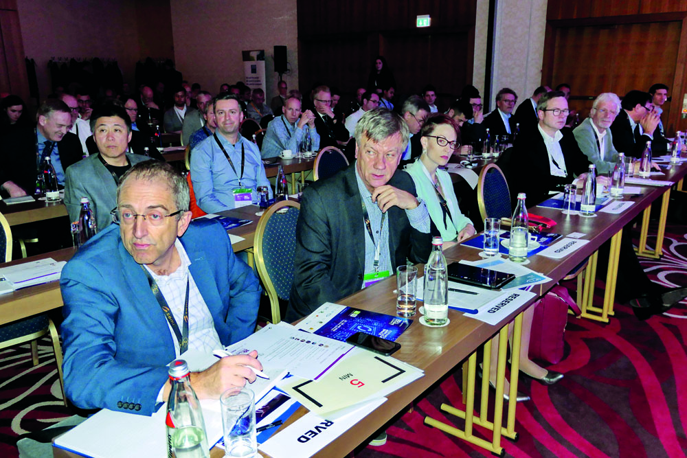
The industry representatives discussed how chips can be connected even more effectively in 3D, what opportunities smart systems developed in this way have in the IoT or for 5G mobile communications, which technologies are required, which chip designs are gaining acceptance and how entire systems can be accommodated in a chip package.
Multichip and chiplet modules - highly integrated systems
The President of TechSearch International Inc., a leading global consulting and licensing company for electronics manufacturing and semiconductor packaging, E. Jan Vardaman, emphasized in her opening speech that "a new era for 3D has dawned". She analyzed the packaging trends for applications in the field of artificial intelligence AI, machine deep learning and prediction as well as 5G mobile communications. Séverine Cheramy from the French research center CEA-Leti also emphasized that smart computing is no longer just a question of cloud high-performance computing HPC, but is essential for distributed computing and AI in smart sensor or smart vision systems with extreme energy efficiency. This development will give rise to new hierarchies for IT and AI: smart hierarchies for combined storage/computing technology for immense volumes of data and efficient edge-to-cloud communication.
There are no standardized solutions for the construction of 3D stacks and multichip modules. In addition to direct assembly and 3D stacking on the basic substrate (PCB core) with flip-chip BGA, flip-chip CSP or fan-out, also on additional intermediate carriers (interposers), stacking at chip level (die-to-die interconnects) or embedding EMIB (embedded multi-die interconnect bridge) are also implemented. Modules with the smallest form factor (System-on-Chip SoC), larger (System-in-Package SiP) and large SiP systems with 100 and more components are possible by adding interposers. This design enables 2.xD and 3D package architectures with mechanical stability and fan-out capability. Routing (rewiring) in 2.5D architectures is done in interposers with through silicon vias (TSV) or embedded bridges. There are now alternative high-density solutions, such as organic fan-out interposers, hybrid substrates, cast molded parts or monolithic vertical 3D interconnect technology with face-to-face placement of active chips. Direct copper-to-copper pad diffusion connections can reduce the pitch to less than 10 µm. Combinations of 2.xD and 3D technologies, heterogeneous 3D integration and the high interconnect density of hybrid bond technology offer many new possibilities.
Concepts such as active interposers or chiplets with high-density hybrid bonds (wafer-to-wafer, chip-to-wafer), high-density TSVs and monolithic 3D bonds with heights of around 100 nm are currently maturing. The so-called chiplets, to which fabless companies have recently switched, are independent functional circuit blocks with mostly reusable designs from different suppliers that work together in a complex multi-chip system.
Mustafa Badaroglu from Huawei Technologies Deutschland GmbH Dresden emphasized that mobile applications are characterized by More Moore scaling, clock frequency scaling, fine-pitch 3D stacking and investment expenditure. In face-to-face configuration, improved shielding and opportunities for miniaturization and cost reduction, highly integrated SiP technology is well suited for packaging mobile applications or compilers for memory-centric computing, noted Romain Freux (System Plus Consulting). Technology trends for wearables, mm wave (medium and HF, 5G to sub-6G or unlicensed bands) or RF front-end modules or SiP applications for Forecast by Air standards, in mobiles, for 60 GHz radar and for side protection (FO-WLP technologies) were examined.
3D and heterogeneous system integration - market analyses
The 3D summit with participants from all over the world showed how interconnected our world is. This is an advantage when it comes to cutting-edge technologies, the implementation of which requires billions in investment and which only become profitable through high-volume applications. This can only be achieved in a globalized world economy based on the division of labour. But the crisis has also shown how vulnerable the system is. The market analyses presented at the summit were produced before the outbreak of the pandemic. The growth rates of up to 8% estimated at the time are therefore perhaps illusory (or still real?). However, 3D integration technologies are still driving the advanced packaging business. These are changing the world because the value share of semiconductor packaging in the total value of the device is continuously increasing in parallel with PCB/substrate and CMOS development. The technology is penetrating many computer products and making high-performance computing (HPC) for data centers or cloud computing possible in the first place. The developing electric powertrain market will boom rapidly. Electric vehicles require five times more electronics and hybrid technology even seven times more. The development of driver assistance systems (ADAS) for the feet-off, hands-off, eyes-off and mind-off stages plays a particularly important role here. Challenges for heterogeneous integration are control systems, camera modules (complete as 3D systems with embedded control electronics), image processors (SoC) or inertial sensors (3D SiP technology).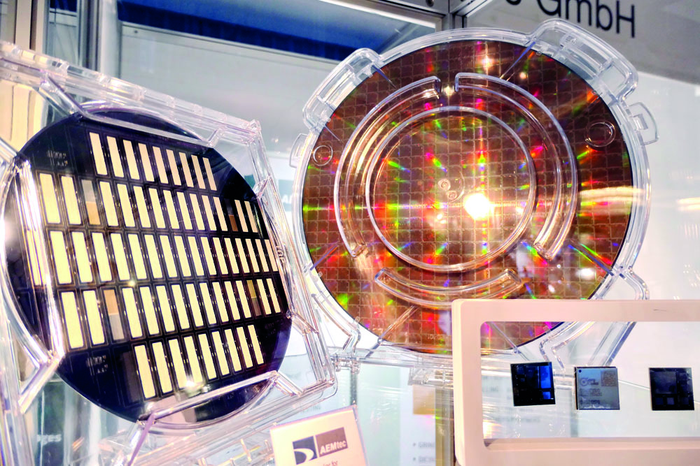 Wafers with high-density microball arrays and Si interposers from the specialist for packaging and wafer backend services AEMtec GmbH
Market developments for heterogeneous integration and the technology roadmap were presented by Emilie Jolivet from French market research, technology and strategy consultancy Yole Développement, Moyra McManus from ASML, Jean-Marc Yannou from the ASE Group and Eelco Bergmann from Advanced Semiconductor Engineering Inc.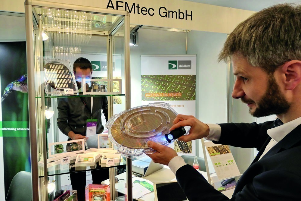 Daniel Lieske shows the tiny TSVs with a magnifying glass
Sophisticated technologies
Function-optimized wafer technologies lead to complex multi-chip packages with high speed and high interconnect density between the tools, because standard BGA substrates are not able to achieve the required I/O pitches for such dense chip-to-chip connections. Bernd Waidhas of Intel Deutschland GmbH Dresden says that PCB/IC substrate technologies developed to date offer a versatile toolbox for the assembly and interconnection technology of multifunctional modules. Current technology development is proceeding along three axes:
- 3D-IC (performance, power,form factors, functionalities)
- Scaling (extensive lithography, new materials and memory technologies)
- Domain-specific architectures (software/hardware co-design, virtual prototyping).
A sensational bridging technology from the Swiss ZeroEC (development center in Tel Aviv/Israel) for 2.5D chip-to-chip was presented for the first time. Data is transported in the "physically most effective way" without energy consumption and with a much higher bandwidth, explained Daniel Graf. "This patented technology, which does not require an electrical conductor, enables the biggest revolution in data transmission since the discovery of fiber optics and ushers in a new generation of IT products." The connection technology is more cost-effective than Si interposers and achieves a data capacity of 10 Gbps (interposer 1 Gbps) with a bandwidth of 25 Tbps/mm (interposer 1 Tbps/mm).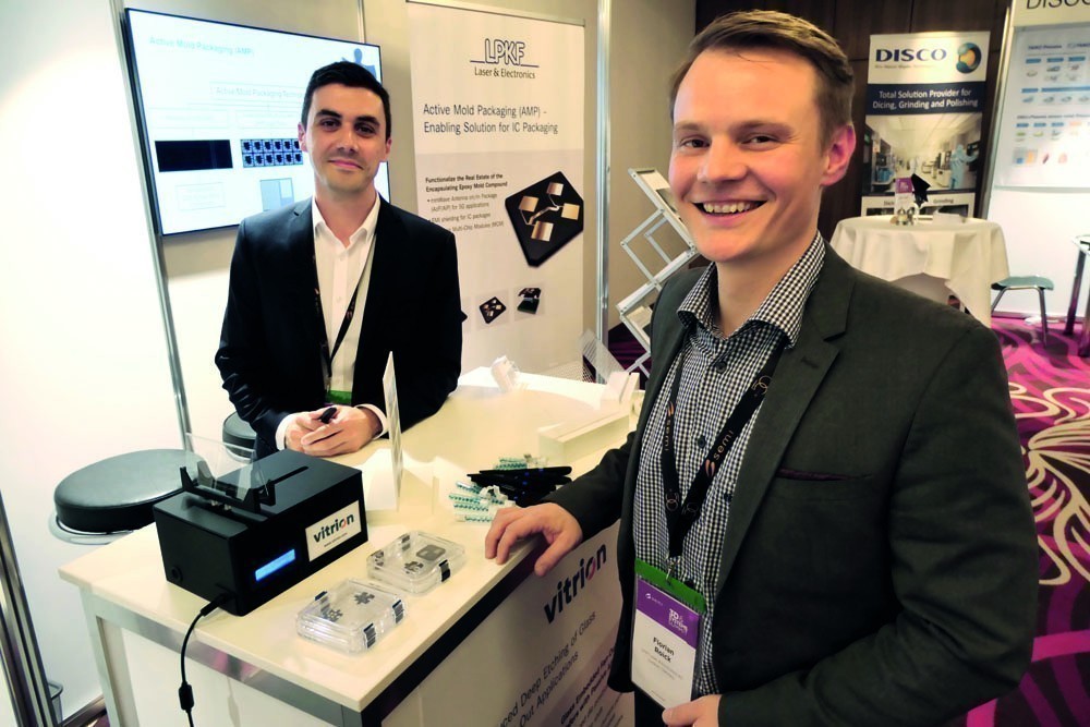 Rafael Santos and Florian Roick presented new PCB prototyping technologies from LPKF
For heterogeneous 3D packaging, 2.5D technologies or the chip embedding technology ECP from AT&S AG either pre-form cavities and then contact the chip (chip last) or stack several wiring layers with fan-out bonded chips at wafer level in chip first and contact them via TSVs (all-in-one packaging). Both technologies can be combined.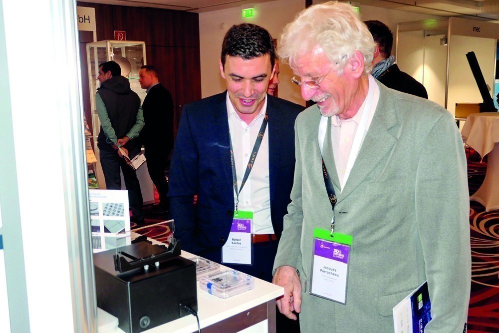 Rafael Santos, here with Jacqes Perrocheau from LCP'S Engineering/France, gave a presentation on new FO technologies
"The development of new classes of materials with superior functionalities are essential to enable new process schemes for wafer and panel level packaging" emphasized Kimberly Arnold (Brewer Science Ltd. USA). New back-end-of-line (BEOL) and front-end-of-line (FEOL) technologies, new interposer technologies and chip-to-chip design approaches were explained.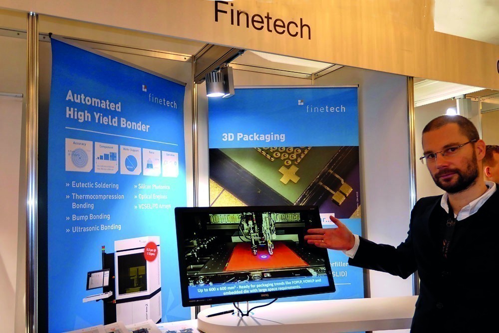 Ralph Schachler explained a multichip bonder from Finetech GmbH Co. KG for large-area (max. 600 x 600 mm) wafer and panel packaging (FOPLP, FOWLP, chip embedding)
Eric Beyne from the Belgian IMEC presented interconnects with pitches up to 100 nm / density up to108 #/mm2. Improvements in system performance and cost are possible through backside power, reduction of FEOL cabling, reduction of dynamic IR VDD/VSS losses and backside decoupling capacitors (PDN noise reduction) at package level. The FEOL or BEOL processes will be less expensive than 2.5D/3D designs with interposers, but do not always support the technical requirements. Amkor Technology Inc. offers a whole range of wafer-level platforms. Low-density fan-out is the extremely flexible workhorse and the most produced WL package with 10 billion units.
Rafael Santos (LPKF Laser & Electronics AG) explained the Active Mold Packaging technology (2.5D) for Mold Fan-Out packages, a laser-assisted functionalization and selective electroless copper plating of LDS epoxy mold material (Laser Direct Structuring). Laser-induced deep-etched or drilled thin glass substrates are also used.
Ruurd Boomsma from BE Semiconductor Industries N.V. in the Netherlands believes that current bonding technologies such as thermocompression bonding need to be further developed and back-end tooling for 2.5D and 3D needs to be taken to the next level of accuracy and productivity. New technologies such as direct bonding are very attractive, but require precision and above all cleanliness, which is why back-end systems need to be upgraded to FEOL technology class systems. zGlue Inc. uses an active (programmable and smart) integration platform ZiP, in which chiplets are assembled in the z-direction by bonding.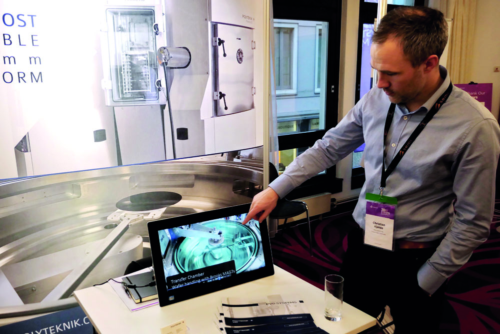 Christian Kjelde from Danish Polyteknik AS presented a flexible PVD processing platform for 200 mm wafers
The lithography systems from Dresden-based ASML Germany GmbH enable scaling at the lowest cost per wafer, explained Steven Stehen, adding: "ASML is creating a new world, currently one nanometer." The semiconductor contract manufacturer Globalfoundries Glofo has further developed a hybrid wafer bonding process for the face-to-face stacking of chips with a hybrid bond pad interface. At the end of April, it was announced that Glofo Dresden had been awarded a certificate for the production of chips with a security level in accordance with the international Common Criteria 3.1 standard by the German Federal Office for Information Security.
Andreas Grassmann from Infineon Technologies AG spoke about virtual prototyping. In April, the Group completed the acquisition of Cypress Semiconductor Corporation, which had been planned since 2019. The acquisition enables the company to offer the industry's most comprehensive portfolio for connecting the real world with the digital world and shaping industrial digitalization.
Heterogeneous system integration in 3D
Miniaturization and integration of different memory, processor or sensor/actuator components leads to functionally more extensive systems and integrated packaging (IP partitioning). Memory chips, processors, sensors, micro-transmitters and other components are stacked in 3D and plated through vertically. Previously unimagined possibilities for scaling, such as 3D imaging devices arranged in the focal plane or neural computing technology, are opening up.
New SoC developments include photonic integration on CMOS on a SiN platform from STMicroelectronics, a packaging concept for a 4-sided gapless sensor from Dectris AG and the heterogeneous integration of 5G components by Fraunhofer-IZM. In April, the Fraunhofer IPMS spin-off Arioso-Systems GmbH received venture capital for the market launch of a microchip technology for a loudspeaker based on a silicon-based transducer principle (nanoscopic electrostatic drive principle).
At the end of 2019, Bosch and Globalfoundries launched the European joint development project 'Ocean12', which aims to develop particularly energy-saving artificial eyes and nerves for autonomous cars or air cabs. 27 European project partners, including TU Dresden and Fraunhofer IPMS, will develop environment sensors for lidar, radar and optical detection as well as microprocessors that translate the collected sensor data directly into control commands for brakes, steering and drive. To this end, sensors and evaluation electronics are each integrated on a single SoC.
The Chinese Joyson Electronic Corp. is relocating its headquarters from Dresden to Ningbo, China, and renamed its previous lead company Preh Car Connect to Joynext GmbH in May. However, Dresden will remain the central R and D location for automotive electronics. The Group wants to "test new ideas even more intensively on the Chinese market, which has a strong affinity for technology", emphasized CEO Yuan Kevin Liu. This market is more important for the company and "the Chinese are more open to new technologies". In addition to Ningbo and Dresden, Joynext includes other Joyson sites in Shanghai and Dalian in China, a factory in Oborniki, Poland, as well as teams in Japan and Korea.
The light at the end of the coronavirus tunnel is getting brighter. It seems certain that Germany has come through the first wave of the global pandemic relatively unscathed. Now the reconstruction begins. Everything that has suffered under the burden of the shutdown in recent months is recovering, if this is possible outside of globalized structures. However, coronavirus is still paralyzing the economy and industry in many countries. As a result, international supply chains are still struggling. In order to stabilize corona-disrupted supply chains, the Dresden network 'Smart Systems Hub' held its first 'Digital Thin[gk]athon' on supply chain management at the beginning of April 2020. Michael Kaiser, Managing Director of Smart Systems Hub GmbH, said: "The crisis also offers opportunities to break new ground together and completely rethink processes. The need to leave well-trodden paths has never been greater."
Sources:
3D & Systems Summit:
www.semi.org/eu/connect/events/3d-and-systems-summit
Silicon Saxony e.V., www.silicon-saxony.de
News portal Oiger, www.computer-oiger.de
