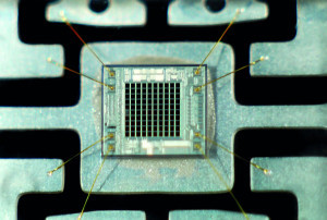
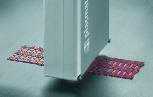
For a long time, atmospheric surface treatment could not be used in PCB production - there was a risk of short circuits. However, with potential-free plasma surface treatment, as offered by Plasmatreat, PCBs can be activated and cleaned over their entire surface or selectively.
 Plasma technology can be used to gently and reliably pre-treat plastic or metal core-based PCBs as well as ceramic and LS switch carriers after die bonding and before wire bondingThetechnology of plasma surface treatment can be used in a variety of ways in the electronics industry, for example in the production of PCBs or semiconductor components - in various process steps, e.g. wire bonding and die bonding, thermal compression bonding and pre-molding. A distinction is made between two different plasma processes: With the low-pressure plasma process, several components can be treated simultaneously with plasma in a vacuum chamber. However, equipment costs and long process times can be a disadvantage with this process. Furthermore, selective treatment of individual components is not possible.
The open-air plasma process developed by Plasmatreat, on the other hand, allows selective and targeted treatment of components. The surface treatment based on one or more nozzles works with compressed air, does not require any cost-intensive gas and can also be flexibly guided by a robot. It is also possible to use open-air plasma in the production process both inline and as an isolated solution. The process is suitable for surface treatments such as ultra-fine cleaning, surface activation and plasma coating of almost all materials such as plastics, metals, glass, ceramics and composites. Openair plasma technology is also suitable for cleaning all metallic surfaces.
It is particularly interesting for the semiconductor industry when a different gas is used instead of compressed air, e.g. special gas mixtures for treating copper. Because this element is extremely sensitive to oxidation, especially at higher temperatures, only low-pressure plasma systems or processes in a protective atmosphere are normally used for this purpose. Reducing treatment with open-air plasma, on the other hand, allows copper lead frames to be cleaned very quickly without any noticeable discoloration of the copper frame. The low thermal stress on the components allows, for example, plastic or metal core-based PCBs to be processed without thermal damage. Ceramic and LS switch carriers can also be treated after die bonding and before wire bonding. Chip damage caused by electrostatic charges is ruled out with the electrically neutral plasma nozzles.
Designed for specific requirements
 Chip packaging can also be cleaned of unwanted oxide layers using open-air plasma and suitable nozzles before further processingThesemiconductor industry has been using plasma products manufactured by Plasmatreat for some time now. However, a request from a long-standing customer prompted the development of a special Plasma Treatment Unit (PTU for short) for the semiconductor industry. "As an established system supplier for our PTUs, we were happy to take on this very specific request," says Nico Coenen, Market Segment Manager Electronics at Plasmatreat. The PTUs are individual production cells that can be seamlessly integrated into production lines and are designed to suit the customer's process engineering workflows. This also includes various handling and automation options that enable coordinated process automation for efficient surface treatment and precise handling of assemblies and components. "As we already manufacture fully automated systems for other industries, we didn't have to build up the internal design and automation expertise required to develop and implement the system requested by the customer," Coenen continues. "We did, however, expand our testing capacities at the Steinhagen site and set up a class 6 clean room for this special customer project."
Plasmatreat developed this system specifically for the semiconductor industry. For example, vacuum clamping devices were integrated to fix the component trays and SECS/GEM-based protocol interfaces were used. "In order to develop an inline-capable system for the semiconductor industry and guarantee the highest possible cycle times, several process steps had to be taken into account during the design phase," emphasizes Coenen. "For example, we planned the parallel handling (dual-lane concept) of two depositing devices on two conveyor belts within one system. We read barcodes in order to be able to trace each chip. We can also treat individual components selectively and, for example, only treat the top side of a component with plasma. This specific treatment is not possible with vacuum plasma, for example."
Maximum throughput
 Anne-Laureen Lauven, Head of Marketing at PlasmatreatThedual-lane concept with adaptation to individual cycle times at the customer is basically designed for various applications. The system achieves maximum throughput per square meter. The system, which is designed for both JEDEC trays and leadframes, can process trays with 8 or 128 components. Furthermore, the barcode of the components transported in a JEDEC tray is read on the fly using a camera in the first step of the PTU currently supplied. This allows each individual component to be traced. In the next step, the components are fixed in the compartments of the JEDEC tray by creating a vacuum. The subsequent surface treatment is carried out using the RD1004 rotary nozzles equipped with an integrated suction unit. Once the plasma surface treatment is complete, the components pass through an external, selective flux module, where they are prepared for the subsequent thermal compression bonding process.
The dual-lane concept (see introductory photograph) allows different processing concepts to be used depending on the cycle time. The first conveyor belt transports two filled trays one after the other to defined positions where the surface treatment takes place. At the same time, the second conveyor belt transports two further loaded trays to the respective processing positions. As soon as the surface treatment of the components on the first conveyor belt is complete, the two plasma nozzles move to the second conveyor belt and process the components located there. As the finished trays leave the system, the next trays move up. Communication within the production line takes place via the standard equipment interface protocol interface in the semiconductor industry, SECS/GEM.
"The electronics industry is repeatedly confronted with a shortage of components," emphasizes Coenen. "Increasing electromobility is not exactly helping to ease the situation either." Plasmatreat therefore also wants to design and implement individual plasma solutions for the automation and mechanical engineering sectors. The aim is to find cycle time-optimized alternatives in the production of chips and microprocessors.


