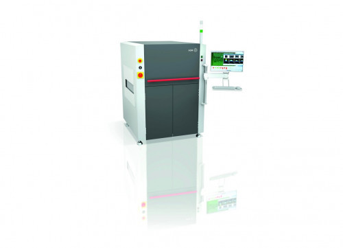
Speed or precision - until now, electronics manufacturers often had to choose between these two parameters when using an SPI system in their SMT line. Thanks to a new HD optical system, ASM has managed to ensure that precision and speed are no longer mutually exclusive.
With the new optical system of the ProcessLens solder paste inspection system, the inspection time is reduced by up to 70% compared to conventional SPI systems with a resolution of 20 µm in high-speed mode. In the only slightly slower high-resolution mode, even 10 µm is achieved. This makes ProcessLens by far the fastest and most precise high-end inspection system in the industry. "ASM thus combines the need for maximum precision in the semiconductor sector with the speed requirements of SMT production," says Jérôme Rousval, ASM Solutions Marketing Manager and specialist for SPI systems.
High-speed meets high-resolution
 ProcessLens is up to 70% faster than conventional SPI systems - without compromising on qualityForexample, the new SPI system only needs 3.0 seconds in high-speed mode and 3.7 seconds in high-resolution mode (resolutions of 20 or 10 µm) to inspect a standard board with an area of around 69,000 mm² and more than 6020 depots.
At 50 x 50 mm (2500 mm²), the scanning area of the 25 megapixel camera is 277% larger than in the previous version with 4 megapixels and 30 x 30 mm. The number of micromirrors in the DLP chip (Digital Light Projector) for generating the moiré patterns has been increased from 8 million to 20 million to achieve a much higher resolution. Their size has been roughly halved. Each individual mirror can be controlled electronically so that the stripe patterns can be projected without any movement of the light source and without vibration or deviation.
The ability to switch between high-speed and high-resolution mode under software control opens up a considerable increase in production flexibility. In addition, this provides a high level of investment security: companies are also equipped for future changes in inspection tasks - without costly recalibrations, technician assignments or changes to the inspection programs.
New generation algorithms in use
The DLP chip is controlled by a new generation of algorithms that generate moiré patterns much more precisely and quickly: The time taken to change the position of the mirrors for fringe generation is now an impressive 16 microseconds. In addition, inspection programs can now also be exchanged between machines and platforms. This also applies to important machine properties, such as the rotation of the camera. If these settings are transferred to another machine, the software automatically adjusts them to ensure the same quality of measurement results.
Another focus was on the further development and refinement of the control mechanisms for accurate work in the millisecond range. Vibrations from the moving parts of the inspection system are compensated and the light control is optimized by compensating for delays until full luminosity is reached. ASM has also achieved further improvements in terms of thermal stability. Only when all optical elements of the SPI are insensitive to thermal influences can even the smallest distortions of the recorded images be ruled out.
All elements were manufactured for the reliability test using a 3D printing process. No part manufactured in this way passes the subsequent test unless it achieves a reliability rate of 99%. Heat dissipation was also redesigned for optimum heat management within the machine.
The result of the development work is a drastic reduction in pseudo faults, operator intervention or line stops. With the option of expanding to a system with artificial intelligence including autonomous process control and optimization, ProcessLens can become a prerequisite for the comprehensive automation of SMT production in an Integrated Smart Factory, according to the supplier.


