Hannusch Industrieelektronik in Laichingen organized a technology day to mark its 35th anniversary, at which a brief review of the company's successful history was followed by an outlook on the future of the electronics manufacturing industry. The celebrations also included an open day for a tour of the company and a festive evening.
Since its foundation 35 years ago, the company has continuously developed and has always been one step ahead of its customers' needs. From humble beginnings as a manufacturer of assemblies for writing telephones, the portfolio has been continuously expanded. Today, the company offers a comprehensive range of services covering the entire value chain from design and production according to individual specifications to commissioning, maintenance and repair. Hannusch Industrieelektronik not only produces electronic assemblies, but is also active in switch cabinet and plant construction.
Technology Day - presentations on current challenges and new opportunities
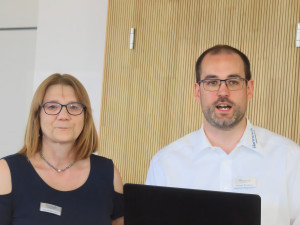
 Claudia and Michael Hannusch welcoming the guestsThecelebrations for the 35th anniversary were opened with a technology day. The topics ranged from printed circuit boards and stencil printing to assembly and soldering to AOI and traceability and were met with great interest. The Technology Day, moderated by Dr. Hans Bell, also provided a platform for the exchange of specialist knowledge and the discussion of forward-looking developments.
Claudia and Michael Hannusch began with a brief review of the company's history before moving on to the current situation. The positive response from customers to the range of services on offer shows that the company is on the right track. Compared to the previous year, turnover increased by over 15% in the first half of the year. Nevertheless, there are still delays in the delivery schedule, as the material situation has improved significantly compared to the previous year, but there are still missing parts and a few other bottlenecks. Further increases are expected, both in terms of order volumes and product diversity, meaning that resources (personnel and equipment) need to be expanded further. A major challenge in expanding capacity is the shortage of skilled workers. Qualified workers are urgently needed.
Experts from the electronics industry then gave the following presentations:
- Dr. Hans Bell emphasized in his introduction that production could not iron out everything, citing the tombstone effect as an example. For this, as for many other problems, an unfavorable design is the main cause.
- Uwe Zimmermann, NCAB, listed the cost drivers for printed circuit boards. The design has a decisive influence on the overall costs and reliability of a PCB. This is why changes are required for practically all new PCBs. NCAB supports this with a free initial sample test report.
- Frank Breer, Christian Koenen, talked about the challenges of stencil printing, including the rules for stencil design and the advantages of stepped stencils.
- Torsten Vegelahn, EKRA, explained what printing in new 'spheres' is. Using the new Serio 6000 printing system as an example, he showed what the path to autonomous stencil printing looks like.
- Thomas Kempf, Juki Automation Systems, showed how profitable optimizations in production can be achieved while increasing quantity and quality. The logistics and transportation of SMDs can now be fully automated, from goods inwards (at the production line) to warehouse (management) and provision for assembly (machines).
- Rehm's portfolio comprises eight processes that offer endless possibilities. Michael Hanke, Rehm Thermal Systems, focused on the SMD soldering and coating systems. The latter, the Protecto, is characterized among other things by intuitive operation via a touchscreen.
- Harald Eppinger, Koh Young, used the Zenith 3D AOI series to explain what a modern 3D AOI system can achieve. The true profilometric shape of components, solder joints, patterns, foreign material on PCBs and more is measured using AI-supported functions and the results are visualized using KSMART, optimizing and standardizing the process.
- Swen Nothjunge from Asys spoke about traceability solutions. The basis for traceability is individual marking, so that identification is possible. He showed that laser marking is an advantageous method for this.
- Dr. Heinz Wohlrabe, TU Dresden, explained the influence of twisting and warping during the soldering process on the quality of solder joints. Due to coplanarity changes of 350µm, for example, the so-called head-and-pillow effect occurs when soldering QFP.
- With regard to the design for selective soldering, Jürgen Friedrich, Ersa, explained what should be taken into account in the layout based on the thermal process window and the solder-dependent soldering parameters. Particularly important are suitable solder gaps and heat traps (which can also be realized as thermal vias).
- Helge Schimanski, Fraunhofer ISIT, used examples of faults - including ESD and press-fit technology problems - and their causes to demonstrate that quality-assured electronics production can be achieved through advanced fault analysis.
Open day and donation raffle
The doors of Hannusch Industrieelektronik GmbH were open for an open day, so that interested parties were not only able to gain an insight into the ultra-modern production facilities, but also had many questions about the processes answered.
In addition to the company tours, a festive evening and a donation raffle were organized to support local social projects such as the BBU'01 wheelchair basketball team and a new skating rink in Laichingen.
The 35th anniversary of Hannusch Industrieelektronik was another successful milestone and provided a glimpse into the future.


