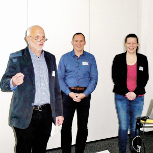
Saxony, and Dresden in particular, is one of the leading centers of the semiconductor industry and electronic device technology. The Saxon Working Group for Electronics Technology (SAET) strives to achieve open cooperation for experts in the field of electronics packaging and interconnection technology through regular meetings in accordance with the work priorities of the VDI/VDE Society for Micro and Precision Engineering.
The 81st meeting of the SAET was organized in the specialist context of 'dresden elektronik ingenieurtechnik', a service provider in the electronics sector. The long-standing connection between the SAET and this company goes back to 2015, when a visit took place to celebrate the company's 25th anniversary. Currently, 'dresden elektronik' employs 110 people who actively contribute to development and innovation in the electronics sector. Since 1990, 'dresden elektronik' has been operating on the market as a partner for complex electronics development and series production.
The business areas of 'dresden elektronik'
The Dresden-based company is divided into three business areas: The E2MS division (Electronic/Engineering/Manufacturing/Service) forms the solid foundation and focuses on contract development and production. The company accompanies its customers from the initial idea through to series production and offers support both in sub-areas and for complete orders - from prototype development to series production.
Daniela Geißler presented store floor management from customer order to production order, material management with supply chains and warehousing as well as the store floor and production planning tools. She discussed how the company maintains an overview of running stores despite possible disruptions and the variety of products and described change management (from KPI to corrective action) in production. The direct interaction between the development and production departments enables fast and flexible product adjustments. Customers benefit from a significantly reduced time-to-market and high-quality, marketable products.
In the radio sector, the company presents a broad spectrum of individual solutions. Particularly noteworthy are customer-specific solutions that specialize in the low power radio standard IEEE 802.15.4 for wireless sensor networks with ZigBee under the established Phoscon brand. Overall, the Phoscon brand stands for innovative solutions in the field of intelligent lighting and building control, with dresden elektronik developing the underlying electronics and technology. These products enable users to seamlessly network and control their smart home devices. The 'dresden elektronik Verkehrstechnik' division specializes in the development of innovative products in the field of display systems and traffic control. Its expertise covers all phases of the product life cycle. The control systems (DFI systems) for traffic management cover the range from pedestrian facilities and small junctions to complex traffic junctions and timetable display systems with e-paper displays. These systems are already in use in various cities in Germany, Austria and Switzerland.
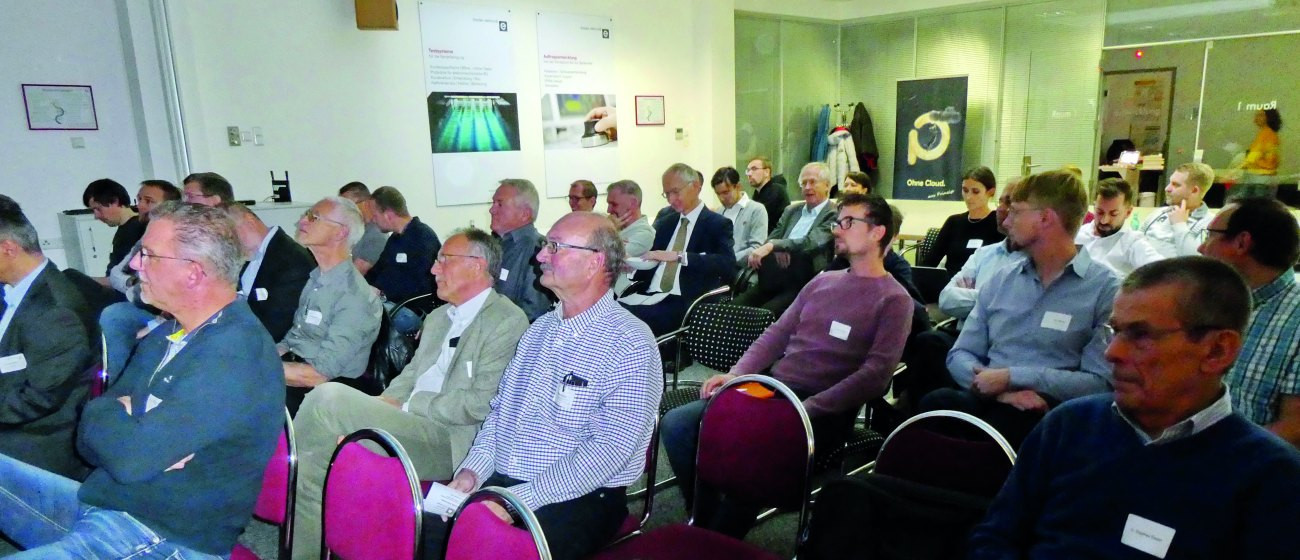 The participants listen intently to the speakers' presentations
Test technology and test automation
 Two AOI, the extensive tester and testing technology, the type testing laboratory and a comprehensive visual inspection ensure quality in productionStefanKempe, responsible for process design at the company, spoke about the highly complex and central topic of testing processes and test accuracy at 'dresden elektronik'. He emphasized that a high level of test coverage can be achieved with a large number of test processes, a prerequisite for stress-free, reliable and reproducible production.
In 2002, the company introduced worker self-inspection for SMD and THT finishes (100%, for Siplace assembly in random samples) and formed a separate quality assurance department. Later, set-up control and an acceptance procedure (dual control principle) were introduced in the siplace line. Organizational solutions for stencils and solder pastes helped to eliminate massive soldering problems. With the introduction of selective lacquering in 2012, process approval lacquer and set-up control lacquer became necessary.
There are two AOI systems, systems for in-circuit, flying probe, boundary scan and function tests, automatic production tests for ZigBee products, for the photovoltaic, automotive and telecommunications sectors. Customer-specific adaptations are developed.
Paperless production with PDA terminals at every workstation was introduced in 2021. Great importance is attached to transparent production, recording test results, traceability and feedback from production employees. The latest achievement is online access for customers, which makes the current status of a customer order visible in production.
Over the past year, low error rates and high first pass yields of 99.7% were achieved in production, 98.8% in Q testing and 99.92% in functional testing for specific assemblies. Essential for achieving such results are the support of the management, control of the processes through organizational and personnel measures, clear contractual regulations of test procedures, anchoring in the assembly technology, detailed work preparation, feedback and, above all, qualified employees with reliable, application-ready knowledge and technological discipline. A practicable modification service and consistent evaluation of customer RMAs are also essential.
Production management
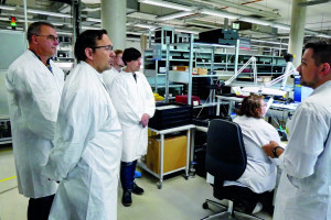 The area for manual production has not become any smaller than in 2015Theparticipants of the meeting were able to see the very well-equipped electronics production facility for themselves during the tour of the plant, as they did during the visit in 2015. New equipment has made the production hall very cramped. Even if there are limits to the networking of production lines and automation, this is not a disadvantage in terms of product and batch size diversity.
Solder paste and adhesive printing is also carried out for SMD and THT or pin-in-hole technologies in both small and large series quantities. At the same time, general connection technologies such as riveting and the processing of press-fit connectors are used. Equipment for wave soldering, convection reflow soldering, automatic selective soldering and, of course, the possibilities for manual, IC and BGA/QFN soldering as well as repair workstations were on display.
THT components are assembled manually. Another feature of the company is its own high-performance mechanical production facility, which also serves the device construction sector. Small devices and control cabinets with 19″ plug-in units are produced in-house, as well as cable production and cabling. The facilities for protective coatings, passivation and paint encapsulation for higher quality and durability of the assemblies were demonstrated. The author found it remarkable that the assembly employees are trained for all systems and processes and can therefore be deployed as required. This avoids personnel-related downtime and stabilizes the production process.
Chip-on-board production in the clean room
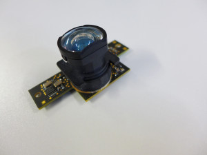 Camera module with mounted optics from First SensorAnotherDresden-based company that manufactures electronic assemblies is 'First Sensor, NL Dresden-Klotsche' (FSP), which the members of the working group have known for many years from various visits as 'Microelektronik Packaging Dresden' (MPD). In 2005, this company was affiliated to 'First Sensor' and is a well-known European sensor manufacturer. Dirk Ensminger, responsible for technology and sensor systems at FSP, now reported on the merger of FSP with the US 'TE Connectivity Corporation', a provider of connectivity and sensor solutions. As a result of the merger, FSP can now serve customers in 140 countries.
FSP has many years of experience and extensive know-how in the development and manufacture of electronic microsystems for components through to microsystems as complex multi-chip modules for the customer-specific miniaturization of optoelectronic and MEMS-based sensors.
The semiconductor chips are processed using state-of-the-art, automated assembly and interconnection technology (AVT) processes. The expertise includes chip-on-board solutions, highly developed technologies for assembly and packaging, customized materials and connection techniques. Special skills exist in the processing of optical sensors, the assembly of large chips (> 10 x 10 cm2) and the processing of chips with TSV technologies. In addition to samples and small series, quantities in the millions are produced.
Dirk Ensminger oversees the implementation of customer requirements in processes for new and current products and presented the core technologies used, from wafer cutting (up to 300 mm) and cleaning, incoming and outgoing inspections, SMD assembly, chip and wire bonding, packaging and encapsulation to optical inspection and electrical testing. For example, chips are assembled in ceramic housings, covered with glass lids, filter glass or lens systems or in a COB process, bonded to printed circuit boards. Assembly must be carried out with the utmost precision and optimized thermal management. Reliability requirements in terms of service life, tested with temperature cycles and storage, are essential.
Key FSP products are camera modules with image sensors for line scan, area or ToF imaging or corresponding boards. The processing of such image sensors requires clean rooms adapted to the various applications, with the exception of wafer sawing and mechanical processing as well as test processes. The company has therefore set up a 2700 m2 cleanroom area, which is divided into ISO class 8 to 5 areas of different sizes. Dirk Ensminger explained some of the company's applications, such as the 'REAL3 3D' and other BGA image sensors. The sensors are used in driver assistance systems, for example.
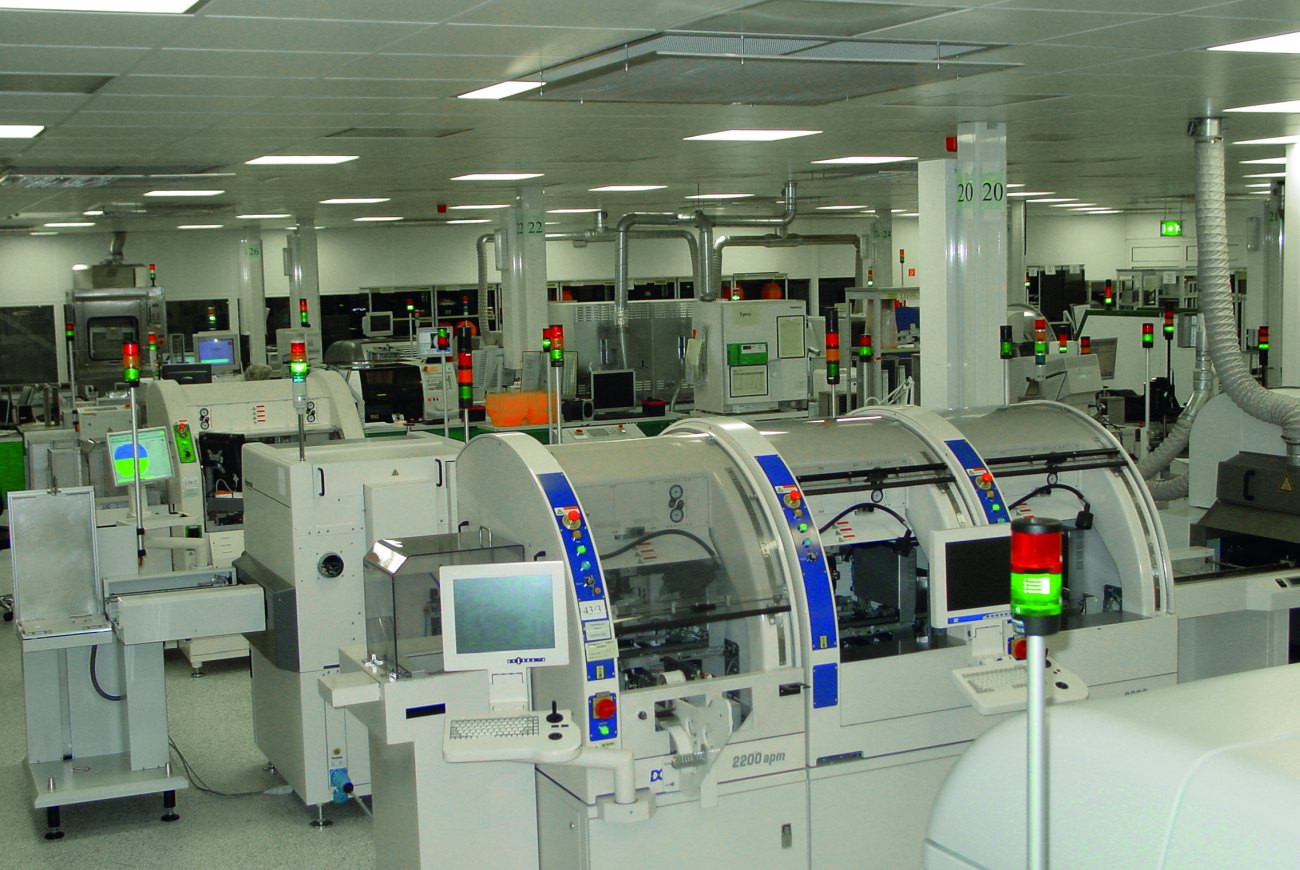 View of FSP's production in the clean room with partial clean room areas
Recycling of waste containing tin and precious metals
Waste from electronics production has always been critical, as it is contaminated with pollutants and high-grade materials. Dan Mutschler from MTM Ruhrzinn Essen therefore explained his thoughts on the recycling of waste containing tin and precious metals. He began with the words: "Imagine we are sitting on sustainable raw materials and nobody is using them!" and mentioned a visitor survey at 'SMT Connect 2022' on the recycling of tin. Respondents were asked about their reservations regarding whether recycled solder is of the same quality as new solder, whether they would use recycled tin of the same quality and whether they would be prepared to pay more for it. 59% had no opinion on this subject, 33% had reservations and only 8% of respondents expressed interest. Of these, only a small proportion were prepared to pay a higher price.
Dan Mutschler described how high-quality solder can be produced from used solder, dross and ash, solder paste residues and contact pins. The ecological balance is very good (< 1 % of energy, 1 %CO2), for gold, copper, lead and silver the ecological balance is similarly good, sometimes better. There are also new processing methods, for example chemical separation instead of the usual thermal treatment for solder pastes. The added value for electronics manufacturers is certified sustainability and optimized electronics production, as well as legally compliant waste management.
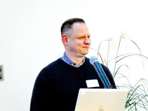 Oliver Albrecht reported on a new non-destructive testing method
Contact thermography - a non-destructive testing method for sintered connections
Following on from Steffan Kempe's presentation, Oliver Albrecht from the Technical University of Dresden, Center for Microtechnical Production, described a new approach to inspecting sintered and soldered connections for chip assembly in power electronics. X-ray radiography and, to a certain extent, ultrasonic inspection are non-destructive testing methods (NDT) suitable for series production of soldered dies. However, there is currently no NDT suitable for series production for sintered connections. Radiation thermography is not suitable. The BMWi ZIM project opted for contact thermography and developed an adapted inspection heater consisting of a heating sensor embedded in a contact stamp and arranged in an automated test stand. This enables a temporally and thermally resolved measurement of the heat dissipation process after thermal excitation by heating (heat flow measurement). An algorithm was developed for rapid evaluation of the heat transfer. Oliver Albrecht presented the fourth generation of inspection heaters and described promising initial results. At this 81st meeting of the working group, the participants were able to follow interesting presentations. This program and a highly interesting tour through the production facilities of 'dresden elektronik' once again stimulated intensive technical discussions. Many thanks to the colleagues from 'dresden elektronik' who made this meeting possible in their company and organized it excellently.
Further information
Saxon Electronics Technology Working Group: avt.et.tu-dresden.de/saet/Arbeitskreis/
dresden elektronik ingenieurtechnik': www.dresden-elektronik.de


