Laser processing of metallized, brittle GaN ceramic substrates is one of the most demanding electronics applications. In this case, this was realized with a ProtoLaser R4 from LPKF.
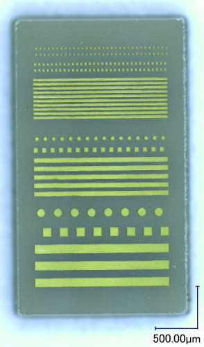
 Fig. 1: The test sample sets new standards in the miniaturization of pattern cut-outs and the resolution of micro-etching the top layer. The outer corners are deliberately roundedGallium nitride substrate(GaN) can be used in power circuits and high-frequency electronics for wireless communication. It is increasingly being considered in place of silicon substrates in the development of power electronics for chips and circuits. Applications include 5G, military and civil aerospace and satellite communications.
However, metallized ceramic materials based on gallium nitride pose a challenge for material processing if a thin metallic conductor layer is placed on a thick, brittle ceramic substrate and both are to be processed with one machine. With the ProtoLaser R4, this can be easily implemented in research and development - both in prototyping and for small series.
In order to process both material layers quickly and cleanly - regardless of the very different material properties and required final specifications - the accuracy, adaptability and tunability of a processing system are required. The R4 was developed for laser processing of new and special materials in research.
With its picosecond laser, it enables the high-precision structuring of sensitive substrates as well as the cutting of hardened or fired technical substrates and is therefore the ideal tool for GaN. The system cuts and ablates the desired materials 'cold', gently and precisely, with virtually no heat input in the adjacent material.
In the laser-based process, two traditionally separate manufacturing steps - cutting the ceramic substrate and etching the conductive layer - can be replaced by a single contactless and chemical-free step. This has been proven in feasibility studies by Dr. Jaka Mur (University of Ljubljana, Slovenia).
The ProtoLaser R4 first cut the ceramic material without cracks or chips and then immediately carried out the microstructuring of the top layer, which in this case was made of gold, without any further user intervention. The laser power and pulse energy were adapted to the specific application.
This process is just one of the many, albeit special, possible applications. The R4 is also suitable for cutting, drilling and structuring typical materials for HF electronics, PTFE, double-sided flexible PCB laminates, thin metal layers on glass, etc. with high precision.


