For almost 20 years, laser direct structuring (LDS) has been used to apply conductor tracks directly to plastic parts in series production. Automated manufacturing processes have recently made the process increasingly attractive in economic terms.
 Dirk Rettschlag is the project manager responsible at the Group subsidiary Harting 3D-MID AG in Biel/SwitzerlandThereis less and less space availableforelectronic assemblies, so solutions are being sought to replace conventional printed circuit boards. LDS enables further miniaturization and increasingly complex geometric designs. The process is process-stable and reliable and has also established itself in particularly quality-critical areas such as medical technology or safety-relevant components for the automotive industry.
The LDS process enables electronic assemblies with flexible geometric shapes. Thanks to this process, electronic products such as smartphones, sensors and medical devices are becoming ever smaller and more powerful.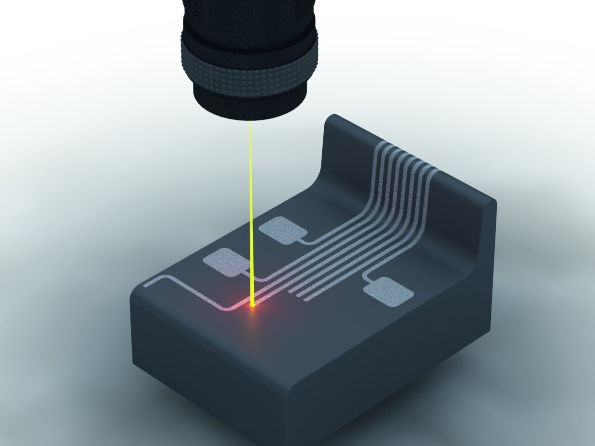 The structure of the conductor track is applied using the LDS process
Consequently, the evolution of laser direct structuring has led to 3D MID assemblies (mechatronic integrated devices). Electronic components are mounted directly onto a three-dimensional base body. Printed circuit boards and connecting cables are no longer required. The base body is produced by injection molding, whereby the thermoplastic material is provided with a non-conductive, inorganic additive.
LDS enables three-dimensional assemblies
The additives in the material are 'activated' by laser direct structuring so that the plastic material can accommodate electrical conductors. The laser beam describes the areas intended for the conductive tracks. The result is a microrough structure. The released metal particles form the cores for the subsequent chemical metallization.
In this way, electrical conductors are applied to the areas marked by the laser. The other areas of the three-dimensional base body remain unchanged. The plastic component can then be assembled like a conventional PCB in standard SMD processes and is also suitable for the soldering process in the reflow oven.
Laser technology can be used flexibly
Harting 3D-MID AG is currently the largest supplier of 3D-MID components outside Asia. For the LDS process, the supplier uses high-performance laser systems with three lasers working in parallel, each offset by 45 degrees. Thanks to the additional axis of rotation, components can be processed by the laser simultaneously from all sides at 360 degrees.
This technology makes flexible geometric shapes possible, such as those required for reflector shells or LED lights. Despite the low conductor track thickness of 16 to 20 μm, the conductor tracks are suitable for demanding automotive components or for applications with currents of up to 10 A - for example, heating coils for cameras that prevent fogging of the optics.
Frequent changes during electronics development or new components with altered dimensions lead to complex adjustments in conventional PCB production. In contrast, the laser layout can be adapted very flexibly by making entries in the laser's control software. Changes in injection molding are not necessary.
Compared to conventional processes, the production of prototypes is also easier with LDS. The plastic base bodies can be produced using LDS-compatible material in 3D printing. Injection molding with cost-effective prototype tools is also used.
New trends in LDS
LDS technology has been improved and further developed in several areas in recent years: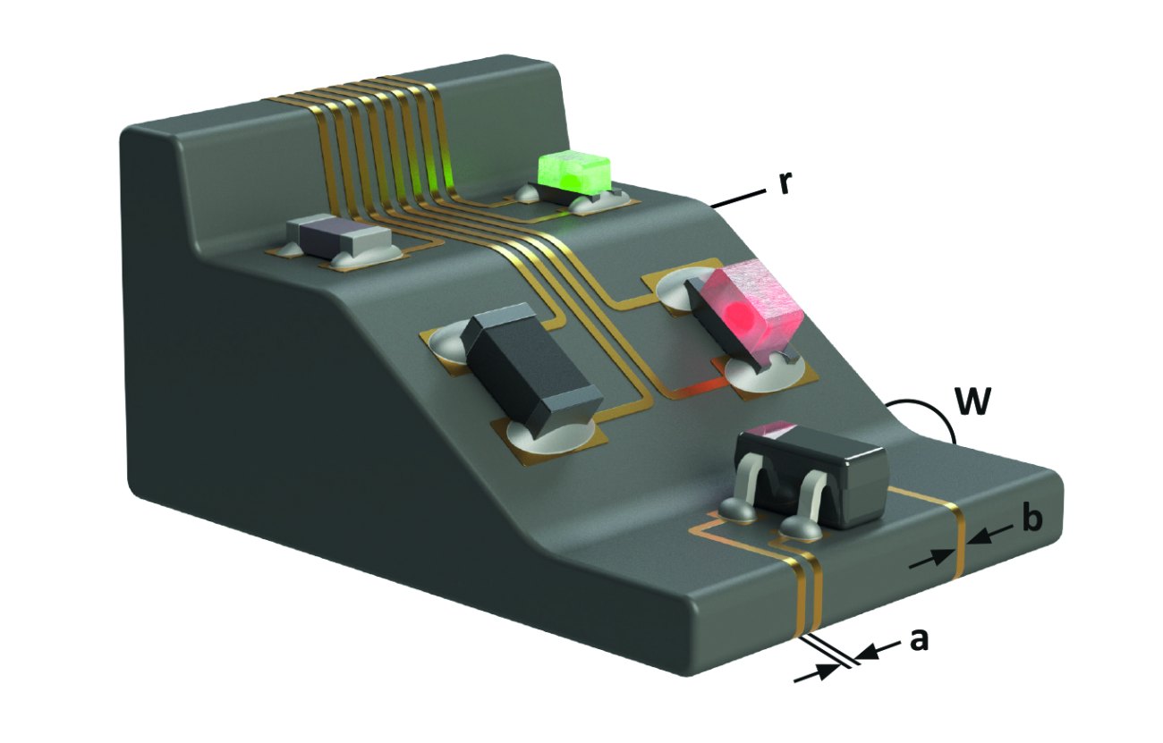 Minimum value for distances between the conductor tracks (a): 150 μm Minimum width of the conductor tracks (b): 150 - 250 μm; radius (r): 0.2 mm
- The working area of the lasers has been increased from 160 x 160 x 80 mm to 200 x 200 x 80 mm, which enables a higher packing density or the processing of even larger parts.
- The working speed of the laser was doubled to 4 m/s by optimizing the servo units and mirrors for guiding the laser beam, thus significantly reducing the processing time.
- In addition to a laser with a diameter of 100 μm, the improved optics also enable a laser with a fine focus of 50 μm for processing even smaller structures.
Harting is currently the only 3D MID manufacturer in the world to have a laser system with three 50 μm fine focus optics. The fine focus laser achieves even smaller conductor track distances. This means that a larger number of tracks can be created on the same component and a higher packing density can be achieved. It is used for safety technology, among other things, because the closely spaced and intertwined conductor paths trigger safety alarms even in the event of the smallest physical interference.
trigger security alarms.
Advances in material and cost-effectiveness
Only selected thermoplastics are certified for the LDS process and are available from stock. Further improvements to the process relate to customer-specific adaptations to the plastic material:
- With the process that Harting uses, non-certified materials are also MID-compatible thanks to LDS additives.
- Color pigments and special LDS additives can be used to achieve specific RAL or Pantone colors for MID plastics.
- By selecting suitable additives, special RF properties can also be created depending on the frequency range.
To further improve the efficiency of the manufacturing process, Harting relies on automation through robot systems. The LDS laser systems are equipped with a rotary indexing table so that a component can be inserted or removed while another component is still being processed. Loading and unloading is automated using robot technology. This increases throughput and autonomy and enables integration into automated production processes. The service provider uses a further automation step in the injection molding process. Here too, a robot takes over the removal of injection molded parts. The use of robots also increases the exact reproducibility of the processes and therefore also improves product quality.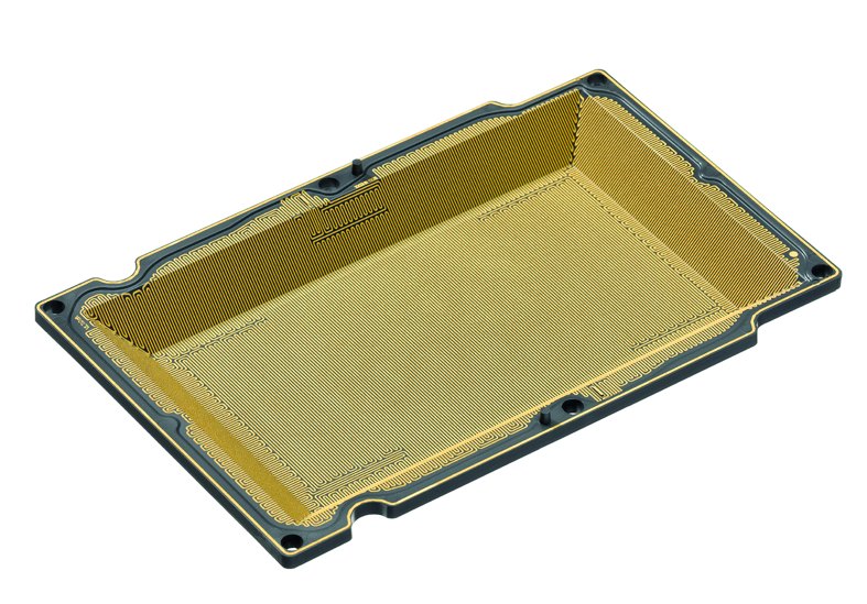
Further growth for 3D-MID
Inquiries for MID projects are currently increasing from many user industries. Harting has therefore further expanded its 3D-MID division by investing in machinery and taking over the business activities of a competitor. Innovative in-house products are also contributing to further growth (see examples).
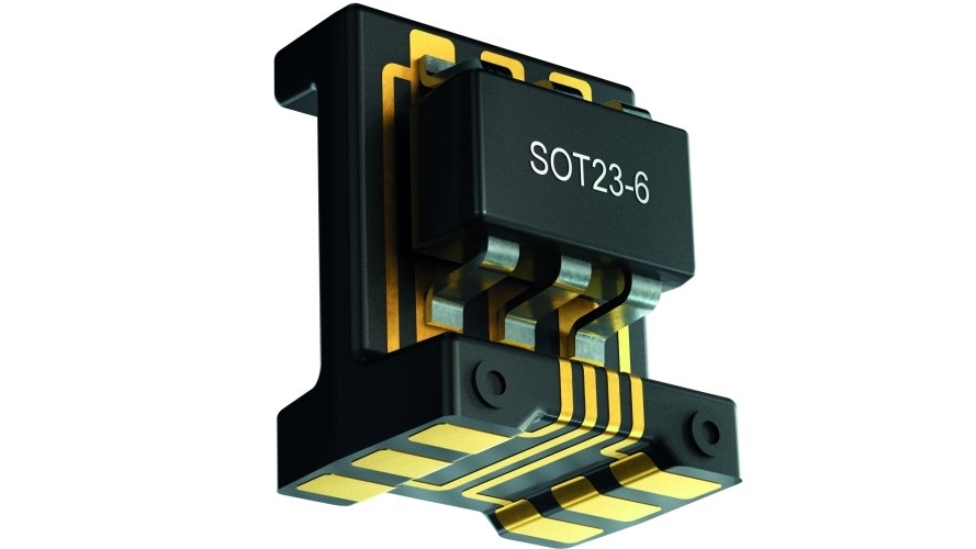
Example 1: Component carriers
Harting has developed the component carrier as a hybrid approach (PLUS 7/2020 p. 950-951): Electronic components such as LEDs, ICs, photodiodes and sensors are fitted directly onto this component carrier. This can then be processed like a standard SMD component (see cover image).
Example 2: Security caps for payment terminals
The security caps protect the reading of credit card information: A high-precision meander structure detects any attempted tampering and thus prevents data theft. The caps, manufactured as 3D-MID components, thus protect the electronics of payment terminals mechanically and electronically against unauthorized access.
