Dear members, friends and interested parties of IMAPS-Deutschland e. V.,
the national chapter of the International Microelectronics and Packaging Society in the Federal Republic of Germany. An eventful quarter lies behind us. After three years of pandemic-related restrictions of various kinds, national, European and international community activities are largely returning to normal. Conferences in particular, as the most important knowledge and technology exchange platforms, can be held in person again.
From February 2 to 3, 2023, our American colleagues in San Diego invited to the "Topical Workshop & Tabletop Exhibition on WIRE BONDING" and many interested parties responded to this call. Thanks in part to our member HESSE Mechatronics, participants were able to find out about the latest developments in wire bonding technologies in the application areas of battery production for e-mobility and sustainable energy, semiconductor manufacturing and microelectronic packaging in various presentations, as well as in the workshop led by Mike McKeown, and exchange ideas in joint breakout sessions.
Wire bonding is still the predominant method of chip connection with a market share of over 85% and offers outstanding advantages over flip-chip technology. Billions upon billions of wire bonds are produced annually. In high-volume and well-controlled facilities, defect rates are in the low ppm range. It therefore remains a cost-effective and, above all, extremely flexible method of chip connection.
In both ball and wedge bonding, the wire between the bonding tool and the bond pad or substrate is massively deformed, creating a welded joint. The dominant variables that influence the deformation are ultrasonic energy, temperature, bonding force and bonding time.
Ultrasonic energy is the main process variable in wire bonding. It reduces the required forces and enables deformation with significantly less stress on the wire and the components to be bonded, such as the chip and substrate, than would otherwise be necessary. High-frequency ultrasound provides higher strain rates and enables faster, more controlled deformation, which is required for precise bonding with high yields and high productivity. This applies to both the widely used thin wire bonding and the increasingly prominent thick wire bonding, as highlighted by Lee Levine in his tutorial.
Other interesting presentations highlighted the challenges but also process variations and solution approaches for thick wire bonding of copper wires, the use of new bonding materials, the requirements for high reliability and failure analysis as well as new test strategies with increasing system challenges and packing densities.
All in all, a very up-to-date program, which was rounded off by around 10 exhibitors in the parallel accompanying exhibition.
Almost building on the content of the conference in San Diego, our French colleagues in Poitier organized a workshop on thermal management from 8 to 9 March 2023, which unfortunately was not as well attended as the topic deserved due to the simultaneous strike of the public administration and the transport system. Research-related, industrial and innovative presentations on the cooling of integrated circuits and packages, advanced materials, thermal management across the entire process chain, from the base material to components, auxiliary and operating materials to the finished product, would have definitely deserved more attention here.
And what can our members expect from us, IMAPS Deutschland e. V.?
After a three-year break, IMAPS Germany resumed its tradition of offering a spring seminar on a current topic in microsystems technology on March 23, 2023. This year, we used various presentations to create a basis for discussion on a pressing contemporary issue relating to sustainability in electronics production: How can we make production or individual production stages sustainable and what aspects must be taken into account?
This topic will be the focus of our reporting in the next issue of PLUS. Stay tuned.
Prototype production of system-in-foil with ultra-thin silicon chips at Hahn-Schickard
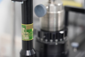
 Fig. 1: System-in-Foil with ultra-thin silicon chip and electrical contacting with inkjet printing (Photos: Hahn-Schickard)Foil-based microsystems with integrated, ultra-thin silicon chips, better known as System-in-Foil (SiF), can be used wherever conventional circuit carriers reach their limits (Fig. 1). Due to their low height, such systems can be integrated into thin-walled structures. This allows, for example, the retrofitting of production systems with sensors ("retrofit"), the functionalization of lightweight elements or space-saving battery monitoring. In aerospace and electric vehicles, SiF can contribute to weight savings. Furthermore, the high mechanical flexibility allows dynamic movements, so that SiF can also be installed in curved installation spaces or used for sensors close to the body and in the form of smart wearables for medical technology applications.
For ultra-thin silicon chips, the back of the chip is removed by grinding. At thicknesses of 50 µm and lower, the crystalline silicon becomes mechanically flexible and can be bent. However, this also makes it more difficult to handle the silicon chips during the process chain from the pick & place process through to adhesive assembly. An unsuitable pick-up of the ultra-thin chips with a suction tool can lead to brittle fracture. Furthermore, the thinned chips are prone to thermo-mechanical stresses due to the structures on the surface, which can cause the entire silicon chip to bulge if it is not constantly fixed during assembly.
The Hahn-Schickard-Institut für Mikroaufbautechnik has developed manual and automated processes for the assembly of ultra-thin silicon chips [1] using adhesive processes. A homogeneous adhesive distribution with a thickness of a few micrometers is achieved on the foil substrates so that the adhesive does not stiffen the bendable chip. After assembly, the sensitive chips were embedded in flexible solder resist using a spray coating to protect them. The solder resist layer, which is only 15-20µm thick, was structured photolithographically in order to open up the contact surfaces on the silicon chip. As a maskless direct exposure process based on UV LEDs was used here, the layouts for opening the contact surfaces and the position of the openings could be varied individually, for example to produce prototypes or to compensate for any twisting of the chips during assembly.
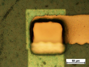
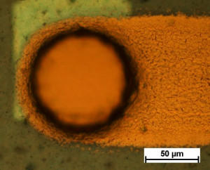
Electrical contacting of the ultra-thin silicon chips is achieved by inkjet printing of nanoparticulate metal inks. Both inks with silver and gold nanoparticles were investigated(Fig. 2). The different solvents of the inks caused different wetting properties, which manifested themselves both as a coffee-stain effect and as a Marangoni effect [2].
 Fig. 3: Foil-based system for characterizing the flexural fatigue strengthIn addition toultra-thin silicon chips, SMDs such as capacitors or resistors are usually also required on SiF. To determine the probability of failure of the contacted components, a bending test bench was set up with which SiF can be dynamically loaded under defined bending radii and with which different metallization layers and contacting methods can be examined.
For example, there was a tendency towards a higher number of bending cycles up to failure with conductively bonded SMDs compared to soldered SMDs [3]. The form factor of the SMD, on the other hand, showed a negligible influence.
Literature:
1. Janek, F.; Saller, E.; Müller, E.; Meißner, T.; Weser, S.; Barth, M.; Eberhardt, W.; Zimmermann, A.: Feasibility Study of an Automated Assembly Process for Ultrathin Chips, Micromachines, 11, 2020, 654, doi:10.3390/mi11070654
2. Janek, F.; Eichhorn, N.; Weser, S.; Gläser, K.; Eberhardt, W.; Zimmermann, A.: Embedding of Ultrathin Chips in Highly Flexible, Photosensitive Solder Mask Resist, Micromachines, 12, 2021, 856, doi:10.3390/mi12080856
3. Saleh, R.; Schütt, S.; Barth, M.; Lang, T.; Eberhardt, W.; Zimmermann, A.: Assembly of Surface-Mounted Devices on Flexible Substrates by Isotropic Conductive Adhesive and Solder and Lifetime Characterization, Micromachines, 13, 2022, doi:10.3390/mi13081240
Calendar of events
|
Place |
Period |
Name |
Organizer |
|
Albuquerque |
18 - 20 Apr 2023 |
3-in-1: CICMT+ HITEC+ PowerPack 2023 |
IMAPS/ACerS |
|
Oslo |
12 - 14 Jun 2023 |
NordPac 2023 |
IMAPS Nordic |
|
Cambridge |
11 - 14 Sep 2023 |
EMPC 2023 |
IMAPS UK |
|
San Diego |
Oct 02 - 05, 2023 |
56th International Symposium on Microelectronics |
IMAPS US |
|
Munich, Germany |
Oct 19 / 20, 2023 |
IMAPS Germany Fall Conference |
IMAPS DE |
|
Munich, Germany |
Nov 14 - 17, 2023 |
SEMICON EUROPE |
SEMI Europe |
This calendar is subject to change. Please refer to the information and notes of the organizers on the respective websites!
IMAPS Germany - Your association for packaging and interconnection technology
IMAPS Germany, part of the 'International Microelectronics and Packaging Society' (IMAPS), has been the forum in Germany for all those involved in microelectronics and packaging technology since 1973. With almost 300 members, we essentially pursue three important goals:
- we connect science and practice
- we ensure the exchange of information among our members and
- we represent the position of our members in international committees.
Imprint
IMAPS Germany e. V.
Kleingrötzing 1, D-84494 Neumarkt-St. Veit
1st Chairman: Prof. Dr.-Ing. Martin Schneider-Ramelow, Director of the Fraunhofer Institute for Reliability and Microintegration (IZM),
Treasurer
(for questions about membership and contributions):
Ernst G. M. Eggelaar,
Detailed contact information for the board members can be found at www.imaps.de
(Board)
Contact:
Mr. Florian Janek
Hahn-Schickard Society for Applied Research e. V.
E-mail:


