IMAPS activities worldwide back to pre-pandemic levels
After three years of pandemic-related restrictions in various forms, community activities are largely returning to normal. Conferences in particular, as the most important knowledge and technology exchange platforms, can be held in person again.
In mid-March, the 19th International Device and Packaging Conference and Exhibition was held in Mountains Hills, Arizona. The 66 exhibitor stands on offer were sold out well in advance and the conference hotel was already fully booked at the beginning of February. With 12 Professional Development Courses, top-class keynote presentations and over 80 specialist lectures, the conference was a successful event for all specialists in the field of electronics packaging.
We are also looking forward to returning to tried and tested formats. The IMAPS Germany spring seminar will take place on March 23 at the TU Ilmenau. Twelve presentations will shed light on the various aspects of the broad topic of 'sustainability' in the electronics environment.
September sees the most important event of the year for the European IMAPS community - the '24th European Microelectronics & Packaging Conference EMPC'. The conference is organized by the UK IMAPS Chapter and will take place at the Genome Centre in Hinxton, near Cambridge. The call for papers is closed and the organizers are working on the conference program on the usual topics Semiconductor Industry Trends, Packaging Technologies, Performance and Reliability, Design & Process Optimization, Markets and Developments, Integration, Materials, Design and Test. We cordially invite you to participate in the EMPC, the early bird registration fee is still valid until the end of May.
Galvanic deposition of aluminum at wafer level for packaging technology
Since 2014, the Fraunhofer Institute for Electronic Nano Systems (ENAS) in Chemnitz has been continuously researching the implementation of the electrodeposition of aluminum for the packaging and interconnection technology of microsystems. Various substrates and applications have been considered. The BMBF joint project 'AioLi' (FKZ: 16ES0329K) laid the foundation for scaling up to wafer level. In this project, the coating of printed circuit boards (FR4), ceramic printed circuit boards in thin-film technology and Al layers for the production of aluminum oxide membranes were investigated. Furthermore, the process was scaled up to 100 mm and later 150 mm wafers. As part of an internal Fraunhofer ENAS research project and a CORNET project (AdEPT; IGF project no.: 200EBG), the electrodeposition process was further developed to 150 mm wafer level. The advantage is that much thicker Al layers can be deposited than in PVD processes and thus the deformability of the Al can be utilized. With these Al layers, wafer-level Al-Al thermocompression bonding (TKB) for hermetic encapsulation and electrical contacting of MEMS and ultrasonic flip chip assembly as a new type of chip connection technology are therefore being researched (Fraunhofer internal, AlPiMon, grant no. SME 601 470). Aluminum offers the advantage that it has very good adhesion and contact with silicon oxide or silicon. A diffusion barrier as with copper layers is not necessary. As a result, a monometallic system can be created that is free of intermetallic phases. This should also increase the reliability of the joining technology.
Al deposition must be carried out from non-aqueous media. At ENAS, the ionic liquid (IL) 1-ethyl-3-methylimidazolium chloride with aluminum trichloride (EMImCl/AlCl3) from IoLiTec GmbH (Heilbronn) is used in a ratio of 1:1.5. The IL is water-sensitive and must therefore be handled moisture-free in a glovebox. Deposition at wafer level takes place in an IL-compatible deposition cell (Silicet AG), i.e. the materials used are not or only very slightly attacked by the IL. This is currently still a laboratory setup, see Figure 1.
 Fig. 1: A) Deposition cell outside the glovebox in open position; B) Deposition cell during filling with IL inside the glovebox; C) Net reaction equations in the IL
Thermally oxidized silicon wafers with a sputtered Al starting layer are used for the deposition. The Al structures are obtained by deposition in a resist mask. First of all, the deposition parameters for an Al starting layer had to be identified, as it was not possible to transfer the known parameters of a gold or copper starting layer. An anodic back pulse is necessary to achieve adhesion and layer growth on the Al starting layer. Furthermore, only low current densities of 5 to max. 7.5 mA/cm² can be used, so that the deposition rate is between 100 and 160 nm/min. By optimizing the process conditions accordingly, layer inhomogeneities of less than 15 % can be reproducibly achieved. ENAS has thus established a unique process worldwide.
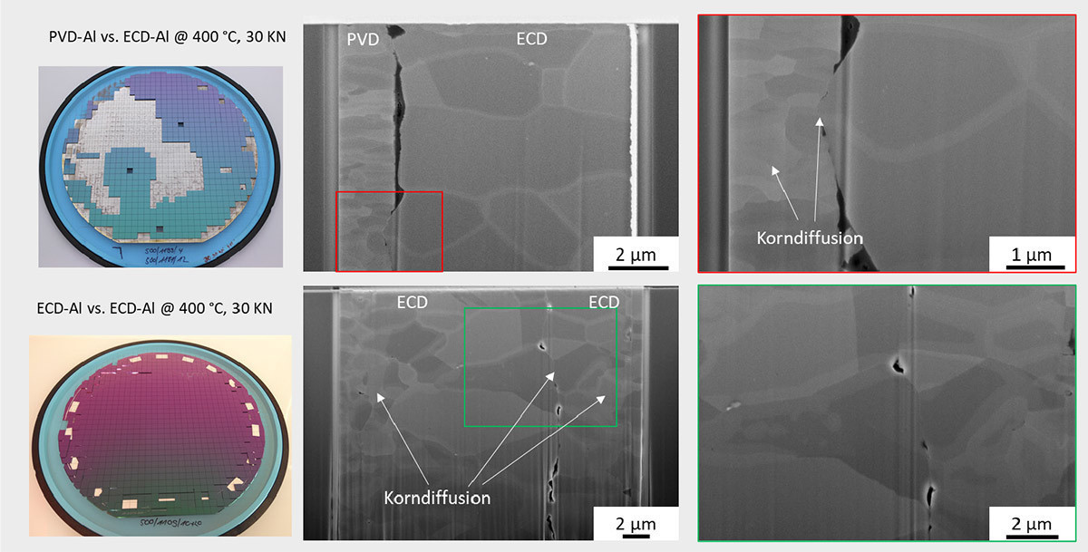
The Al coatings produced are to be used for thermocompression bonding (TCB), for example. TKB is based on solid-state diffusion across a phase boundary. However, the natural oxide layer of the Al acts as a diffusion barrier. Therefore, relatively high forces and temperatures must be used to achieve diffusion between the underlying Al. The electroplated Al layers (hereafter ECD-Al) are not only thicker than PVD layers, but also rougher. These roughnesses could pierce the oxide layer and thus the diffusion barrier, so that lower joining temperatures and forces could be applied. In some bond tests between PVD-Al (2 µm) and ECD-Al (8 µm), it was found that the roughness can pierce the oxide. However, these also act as spacers, so that a closed joint cannot be created. With the same joining parameters but two ECD-Al layers (19 and 8 µm thick), on the other hand, there are significantly fewer defects in the joining zone. In addition, grain diffusion is clearly visible both in the joining zone and inside the coating. The layer composite was compressed by approx. 5 µm, whereas no compression was measurable with PVD-Al vs. ECD-Al. The sawing yield is also significantly higher with two ECD-Al coatings than with PVD-Al vs. ECD-Al. As an example, both results for 400 °C and 30 kN are shown in Figure 2.
 Fig. 2: Comparison of the bond tests for 400 °C and 30 kN for PVD-Al vs. ECD-Al (top) and ECD-Al vs. ECDl-Al (bottom)
For a further understanding of the process, investigations into the process integration of Al deposition, the influence of roughness and the layer thickness must follow.
Furthermore, the deposition method can be used to produce aluminum pillars for chip assembly. The joining process is comparable to an ultrasonic wire bonding process, except that many pillars can be joined simultaneously under the influence of ultrasound. As the aluminium pads of a finished semiconductor chip are used here, no remetallization is necessary, as is the case with solder bumps or copper-tin bumps. The advantage is therefore fewer process steps, fewer intermetallic phase boundaries and therefore potentially greater reliability. This still needs to be proven.
Over the next two years, the electroplated Al deposition process is to be transferred to a fully automated, industry-oriented system so that the processing of 200 mm wafers is also possible.
Contact: Silvia Braun, Fraunhofer Institute for Electronic Nano Systems (ENAS), Chemnitz,
Calendar of events
|
Place |
Period |
Event name |
Organizer |
|
Albuquerque |
18 - 20 Apr 2023 |
CICMT 2023 |
IMAPS/ACerS |
|
Oslo |
12 - 14 Jun 2023 |
NordPac 2023 |
IMAPS Nordic |
|
Cambridge |
11 - 14 Sep 2023 |
EMPC 2023 |
IMAPS UK |
|
San Diego |
Oct 02 - 05, 2023 |
56th International Symposium on Microelectronics |
IMAPS US |
|
Munich, Germany |
Oct 19 - 20, 2023 |
Fall Conference |
IMAPS DE |
|
Munich, Germany |
Nov 14 - 17, 2023 |
SEMICON EUROPE |
SEMI Europe |
IMAPS Germany - Your association for packaging and interconnection technology
IMAPS Germany, part of the International Microelectronics and Packaging Society (IMAPS), has been the forum in Germany for all those involved in microelectronics and packaging technology since 1973. With almost 300 members, we essentially pursue three important goals:
- we connect science and practice
- we ensure the exchange of information among our members and
- we represent the point of view of our members in international committees.
Imprint
IMAPS Germany e. V.
Kleingrötzing 1, D-84494 Neumarkt-St. Veit
1st Chairman: Prof. Dr.-Ing. Martin Schneider-Ramelow, Director of the Fraunhofer Institute for Reliability and Microintegration (IZM),
Treasurer
(for questions about membership and contributions):
Ernst G. M. Eggelaar,
You can find detailed contact information for the members of the Executive Board at www.imaps.de
(Executive Board)


