
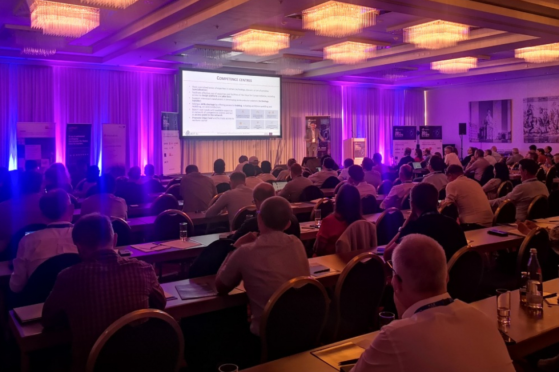
The market for advanced 2.5D and 3D packaging technologies will grow at an above-average rate in the coming years. This was predicted by semiconductor experts at the international conference 'Smarter Systems Through Heterogeneous Integration' organized by the industry association 'Semi Europe' in Dresden.
Semiconductor research director Emilie Jolivet from French market analysis company Yole assumes that the market for chip packaging will increase from a turnover of USD 44.3 billion in 2022 to USD 78.6 billion by 2028 - with annual growth rates of around 10%. In the submarket for 2.5D and 3D packaging, however, annual growth rates of around 30% are expected. However, the top segment in particular has so far been dominated by just a few players. These include TSMC, Samsung, Intel, Hynix and the Chinese group YMTC, which is little known in this country. Amkor, UMC and other companies are also involved in somewhat simpler transition technologies (2.5D).
Europe, on the other hand, is also researching 3D, 2.5D and chiplet technologies, for example at Imec in Belgium, CEA-Leti in France and the Fraunhofer institutes Assid and EAS in Dresden. However, there is no mass production of its own in the 3D packaging segment in Europe. Incidentally, the 'European Chips Act' is also attempting to close this gap to some extent.
"3D architectures will push the boundaries of what is possible, especially for artificial intelligence"
Emilie Jolivet, Semiconductor, Memory and Computing Division Director, Yole Group
 The Fraunhofer Assid Center also presented wafers with 3D-integrated circuits on the fringes of the Semi conference in DresdenGainingground in the 3D integration of heterogeneous circuits and chiplets is increasingly becoming a key topic in the debate on digital sovereignty and competitiveness of competing high-tech locations worldwide.
"Heterogeneous integration promotes the next growth steps in the semiconductor industry," says Vice President Rozalia Beica from AT&S. She even anticipates a whole "new era of microelectronics". And Heiko Dudek from Siemens EDA is convinced: "The advantages resulting from the heterogeneous integration of chiplets will lead to a dramatic increase in demand in more and more markets and applications."
Background: While in the early days of microelectronics, Moore's Law, according to which the transistor density in circuits doubles approximately every one and a half years, was still quite easy to comply with, this path to more computing power has now become extremely complex and expensive. All of this has shifted the focus of the industry away from the core processes of chip production (front end) towards new packaging, contacting and final assembly technologies (back end or packaging) for circuits, towards concepts such as 'chiplets', 3D and 2.5D integration. For example, different circuits, sensors, analog elements and other functional blocks are assembled close together or on top of each other, plated through and then packaged in a housing like a computer chip. These can be one or more central processing units (CPUs), graphics processing units (GPUs), but also memory and communication components. Examples include AMD's 'Ryzen', Intel's 'Meteor Lake', Apple's 'M1 Ultra' produced at TSMC and the Chinese crypto miner chip 'Jasminer X4'.
Higher yield with smaller individual dies
In some cases, the cost issue is central to the use of such technologies. This is because the 2.5D or 3D-integrated function blocks for a chiplet do not all have to be manufactured in the same expensive cutting-edge process. Some can be produced in less expensive, less highly integrated production lines. In addition, smaller dies also increase the yield compared to large monolithic circuits. And in most cases, the aim is to pack more computing power or functionalities into the smallest possible space.
Hybrid bonding' is becoming increasingly popular for particularly high packing and contacting densities in small pitches below 10 µm. In this process, the still unpackaged circuits ('dies') are linked via copper bales ('pads') embedded in silicon. However, Emmanuel Ollier from the French large-scale research center 'CEA-Leti', which is also experimenting with self-organizing structures, emphasized that high-precision assembly techniques are required in order to contact dies or functional blocks on top of each other. He is convinced that the placement and contacting of individual circuits on processed wafers (die-to-wafer) using hybrid bonding is the next big step towards high-performance computing technology based on heterogeneous chiplets.
Industry targets sales in the trillions
 Laith Altimime expects strong industry growth in the coming yearsThe fact thatthe industry is currently putting so much energy into this topic is not least due to the - beyond all periodic fluctuations - constantly growing long-term demand from more and more industries for ever more powerful microelectronics. Semi-Europe President Laith Altimime had already pointed this out at the start of the conference in Dresden: New digitalization pushes in numerous sectors of the economy, the switch to electric cars, the trend towards autonomous driving and numerous government aid programs for chip factories worldwide will remain the most important growth drivers for the global semiconductor industry for the time being, Altimime emphasized. Global microelectronics sales are expected to roughly double by 2030 - from the current figure of around USD 500 billion to over USD 1 billion.
In Europe in particular, strong market impetus is currently coming from the government. Altimime refers in particular to the 'European Chips Act', with which EU Commission President Ursula von der Leyen (CDU) aims to more than double the European semiconductor industry's current market share of 7-9% (estimates vary depending on the analysis) to 20% within a decade.
However, the industry is also facing considerable challenges. These include the shortage of skilled workers: if the semiconductor industry really wants to achieve the trillion-euro sales target by the end of this decade, it will need around one million additional microtechnologists, chipmakers, mechatronics technicians, engineers and other specialists worldwide, predicts senior director Chris Jones from British chip plant supplier 'SPTS Technologies'.
Sources
3D & System Summit Semi 2023, Semi Europe, Yole, AT&S, Fraunhofer EAS, Cea-Leti, Siemens EDA, Oiger.de
 About the person

Heiko Weckbrodt is a journalist and historian. He runs the Dresden-based news portal Oiger.de, which focuses on business, science and innovation policy in Saxony. He also writes guest articles for newspapers and magazines.
