Heterogeneous chip integration based on advanced packaging (AP) technologies is seen as the key to meeting future system performance requirements. This requires increasing value retention, but also means an enormous need for individual customer specification. Yole Développement has conducted a study on this: It forecasts an AP market volume of $47.5 billion by 2026 and growth of the 'traditional' packaging market to $50 billion.
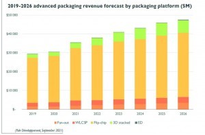
 Fig. 1: Advanced packaging revenue development in USD million, broken down by platform used by 2026Withthe emergence of demanding application fields and technology drivers - big data, artificial intelligence, 5G, high-performance computing (HPC), AR/VR/MR (artificial/virtual/mixed reality), cloud/edge computing, IIoT (Industrial Internet of Things), self-driving vehicles, Industry 4.0 and hyperscale data centers - the semiconductor industry is facing major challenges in designing its components to meet demand. The new applications create potential demand for systems and subsystems with high computing power and high bandwidth with low latency and low power consumption. Added to this is the growing functionality of the systems with greater memory space and support for various sensor classes. Simple integration at system level with simultaneous cost reduction is another requirement of users.
The most important advanced packaging technologies are Chiplets for heterogeneous integration, WoW (Wafer on Wafer) for 3D Nand memory, HBM (High Bandwidth Memory) with 12 or 16 levels of die stacking with pitch scaling to 35 µm, 3D SoCs (System on Chip) with hybrid bonding (logic/logic and memory/logic), stacked 3D ICs for computing systems in data centers and for high performance computing. This leads to large-volume housings (100 x 100 mm2), especially for AI systems, HPC and data networks. And it requires innovative packaging solutions for mobile 5G millimeter wave systems, double-side molded BGAs (ball grid arrays), antenna materials with low dielectric losses, AiP (antenna in package) configurations and more. The further development and adoption of high-density fan-out for all-side-molded WLCSP (wafer-level chip-scale packaging) is expected to accelerate, especially for mobile devices and HPC, such as chip-load fan-out with RDL (redistribution layer) interposer.
Advanced packaging trends
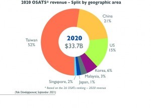
 Fig. 2: OSAT sales in the AP segment in 2020 by world regionIntheir latest study 'Status of the Advanced Packaging Industry 2021, Market & Technology Report - September 2021', three senior analysts (Santosh Kumar, Favier Shoo and Stefan Chitoraga) from French market researcher Yole Développement look at the industrial dynamics, technology drivers and future applications of advanced packaging, a promising trend in semiconductor manufacturing. They break down the expected market opportunities, possible obstacles and disruptions to development, and they draw up roadmaps of front-end scaling and functional enhancements to systems over the next five years. Finally, they outline the positions of the dominant vendors and service providers (IDMs, OSATs, foundries) and their fluid business models.
According to Yole, the AP market reached a global sales volume of USD 30 billion in 2020. It is expected to continue growing at average growth rates of 8% and reach a value of USD 47.5 billion in 2026. For 'traditional' packaging, Yole forecasts average annual growth of just 4.4% to USD 50 billion in this period. Both segments combined will achieve a growth rate of 6 % to USD 95.5 billion. The share of the AP segment is likely to increase to around 50% by 2026. In terms of wafer starts with a diameter of 300 mm, traditional chip packages currently dominate with a market share of 72 %. The profit margins of the AP segment are roughly double those of traditional packaging, which is quite attractive for manufacturers. Flip chips currently account for the largest share in terms of AP technologies used. According to Yole, their share is expected to rise to 80% of the AP market by 2026.
Another advanced packaging platform undergoing dynamic development is 3D/2.5D chip stacking technologies and the fan-out concept. They will achieve annual growth of 22% and 16% respectively by 2026, as their use in future applications becomes more widespread. Fan-in wafer level packaging (WLP) as a direct chip interconnect will grow at an average rate of 5% over the next five years. So far, the WLCSP share of the overall market is still quite modest at USD 51 million. However, it is driven by embedded applications in the infrastructure, automotive and mobile communications sectors and is expected to achieve average growth rates of 22%.
Overall, the Yole report provides an overview of current market and technology developments as well as an analysis of the various global supply chains with the positioning of suppliers and their expansion strategies along with an estimate of their wafer capacities and profit prospects. In addition, there are forecasts for the expected quantities of AP platforms in the various applications in the period up to 2026(Fig. 1).
Provider structure of AP solutions
Equally interesting is the study's assessment of the structure of providers of advanced packaging solutions. These are essentially the OSATs (Outsourced Semiconductor Assembly and Test), but also the large foundries and even the traditional IDMs, which see opportunities in the high-end AP sector. According to Yole, OSATs currently dominate the AP market with a 70% share, measured in terms of the number of wafer starts(Fig. 2). However, especially in the high-end (2.5D/3D stacking, high-density fan-out, etc.), the large foundries such as TSMC and IDMs (integrated device manufacturers) such as Intel and Samsung hold substantial market shares. They are making targeted investments in AP technologies and are working on shifting packaging from the substrate to alternative Si wafer-based platforms.
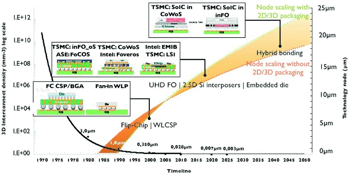
 Fig 3: Roadmap of packaging technology development from 1970 to 2050
As Yole has determined, TSMC, for example, achieved a turnover of around 3.6 billion dollars in the AP segment last year. The investment volume (CapEx) in 2021 amounts to USD 2.8 billion for the development of SoIC (small-outline integrated circuit), SoW (chip on wafer), InFO (chip first) and CoWoS (chip last) platforms and product lines. At Intel, the investment is targeting various AP product portfolios such as Foveros, EMIB and Co-EMIB as part of the recently announced IDM 2.0 strategy as a route to new leadership positions in the semiconductor industry in the area of data center applications. Samsung is also aggressively investing in AP technology to further differentiate itself from TSMC. An overview of the historical development of packaging technologies is shown in Figure 3.
Of course, OSATs are also stepping up their efforts to use innovative AP technologies. At Yole, it is estimated that OSATs have already increased their capital outlays by up to 27% for 2020, which has contributed to their good performance despite the negative impact of the Covid-19 pandemic. In addition to OSATs and IDMs, other players from the assembly business, such as substrate and PCB providers and EMS (electronic manufacturing service) companies, are now also entering the field of advanced packaging. This has implications for the traditional supply chains of semiconductor manufacturing, which Yole discusses in detail in the aforementioned report.


