
The internet is getting faster: 5G is a thousand times more powerful outdoor data transmission and WiFi-6 is a very similar technology for local indoor Wi-Fi. What does it mean for PCB designers to design devices for this technology or to operate devices in this environment?
Many companies are hoping that the widespread introduction of 5G and WiFi 6 will open up new markets. More devices, more sensors and therefore more information that is evaluated, processed and transmitted. It won't just be applications that get by with little data, such as thermostats and heating controls in the home. There will also be more high-resolution video applications in which 4k or 8k images need to be transmitted 'smoothly' in real time. The data volumes here are enormous and defects in the transmission paths will become 'visible' immediately. If sensors are to be used to control traffic, machines and infrastructure, then the transmission link must be stable and a certain transmission performance must be guaranteed.
Improvements are currently being made to the infrastructure in Germany, whereby the Internet backbone is increasingly being equipped with fiber optics (e.g. FTTH fiber to the home). New routers and repeaters then establish the WLAN connection in the 2.4 GHz and 5 GHz frequency band to the fiber optic cable. The ability to connect devices 'wirelessly' quickly and securely will increasingly replace cable connections over the last few meters to the end devices.
There will be two new and similar standards in the future: Outdoor connections will be via 5G and indoor connections via WiFi-6. During the transition period, devices will have to be downward compatible and also support slower standards. As multiple antennas and frequency ranges make the requirements for devices more complex, in a few years there will be many devices, especially in the consumer sector, that only support the new standards.
The advantages of 5G and WiFi 6 are greater bandwidth, more subscribers in a cell, lower latency and more mobility. With a higher bandwidth, video data in 4k or 8k resolution can be streamed easily. This will change the way we watch TV with fixed program times to media libraries with content on demand for streaming. As more participants are possible in a mobile cell, which is also getting smaller, spectators in an event stadium will soon be able to stream the action live to their friends. This will also greatly change the pressure on news broadcasters in terms of timeliness.
The lower latency will also enable the secure control of machines and robots in real time via radio. This will also lead to more IoT devices and more automation in households.
IT architectures will change. If more devices participate in data exchange via radio, the data must be evaluated and corresponding actions calculated for control. In order to control traffic priorities, for example, if the fire department is to be given free passage with flashing blue lights, the status of traffic lights and road users must be recorded, evaluated and controlled centrally. This example alone shows that radio communication must take place in real time and that the large amount of data must be brought together in a central traffic control computer. Nevertheless, the autonomous car must have sufficient computing power to be able to brake in the event of a sudden dangerous situation and also warn other road users in the vicinity by radio. This means that the 5G radio connection must also work for participants in motion.
What do these changes mean for hardware developers?
For future devices, this means that more sensitive sensors will be installed, most of which have analog signals as their source. Suppliers will provide modules with a digital interface or integrate the sensor into an IC package.
Intelligent sensor modules will not only measure data, but also filter and evaluate it according to specifications and make the results available as digital information. Other concepts involve sending digitized data to the cloud, where it is evaluated and processed using artificial intelligence and the results are then transmitted back.
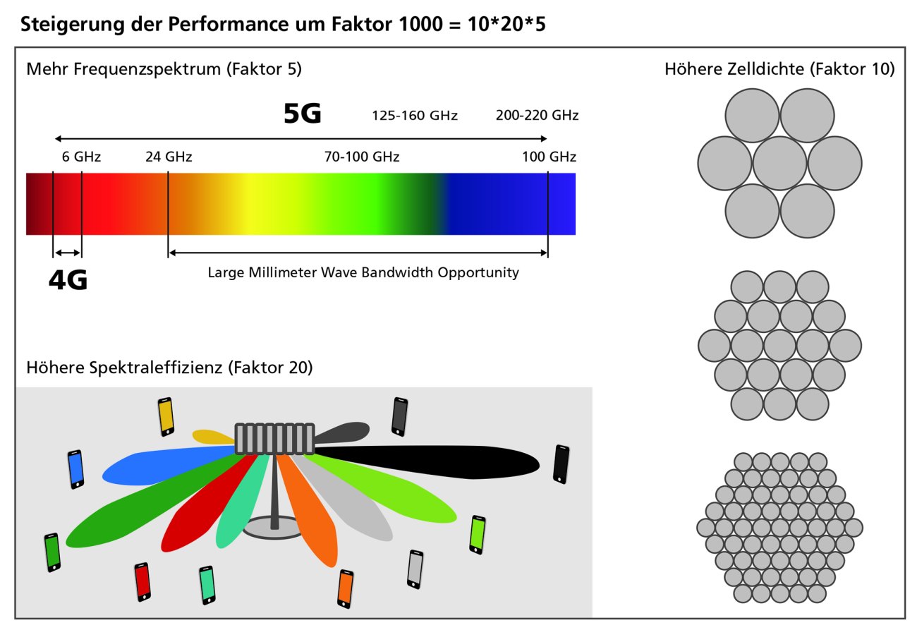 Performance increase by a factor of 1000 = 10 x 20 x 5 with 5G
Simple IoT sensors (e.g. outdoor thermometers) with a long-life battery will only occasionally report measured values to the WLAN. However, if the sensors are part of a local control system, there will also be a CPU or DSP with memory in addition to the antenna in order to control the evaluation and regulation locally and communicate statuses.
The variety of solutions and the complexity of the electronics thus continues to increase. The integration of radio units operating in the GHz frequency band, sensitive analog sensors and digital processors with memories on a printed circuit board poses a challenge in terms of signal quality and EMC behavior. With the simultaneous demand for miniaturization, battery operation and lower power consumption, power integrity and thermal restrictions also come into play.
These issues should not be ignored or put on the back burner. As we have already seen with the last technological leap from 3G to 4G, this leads to a disruption in the previous structure of providers. This is because 3G and 4G not only meant faster data transmission, they also made other business models possible. This gave rise to providers such as Netflix, Google, Apple and Amazon. Other providers that did not take advantage of the opportunities offered by the new technology lost importance or disappeared from the market altogether.
Today, developers need more than just creativity. They should involve the marketing department and let them know what additional benefits can be provided with the devices from the existing data. The market for 5G and WiFi 6 is expanding exponentially and will once again massively change our daily lives.
Technical foundations for 5G and WiFi 6
The enormous increase in transmission speed by a factor of up to 1000 is essentially the result of three approaches:
- Higher radio cell density with more access points per area enables more data throughput by a factor of 10.
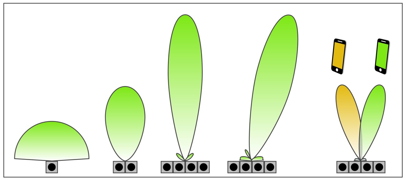
- New MIMO antennas (Multiple Input Multiple Output) can even use beamforming to align the direction of transmission directly to moving objects and achieve a higher spectral efficiency by a factor of 20.
- The additional higher frequencies (>24 GHz) on which data can be transmitted can increase throughput by a factor of 5.
This results in a theoretical 1000 times higher data throughput compared to today's infrastructure.
For semiconductor manufacturers, new materials such as SOI, GaAs and GaN are now being added to CMOS. The quality requirements for SMD components, laminates and IC packages are increasing for the higher frequency applications (5G: 24 GHz - 40 GHz and automotive: 77 GHz - 81 GHz).
GHz on printed circuit boards
New 'air interfaces' with low latency for massive connections can be realized with massive MIMO or patch antennas. For this purpose, transmission lobes are formed from several antennas. Phase shifting results in intentional interference, which makes the shape of the antenna lobes
narrower and amplified by superimposition in one direction. The direction of the antenna lobe can be aligned by controlling the same signal from four patch antennas, for example, with different phases. With the right control, the lobes can also follow moving objects. Instead of distributing a signal to all four antennas in the array, two signals can also be distributed to two pairs of antennas. This allows two devices (WiFi 6) or cars (5G) to communicate simultaneously on the same frequency in different directions without the signals interfering with each other. This increases the power density.
Challenges for antennas
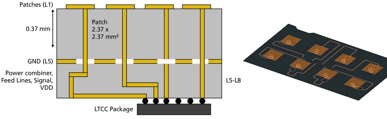
In order to connect antennas together to form an array, the geometric arrangement of the antennas must be absolutely precise. Then the transmitting lobes can be aligned homogeneously in space. Not only do the geometries of the antennas have to be the same, the feed lines for the signals also have to be tuned for high frequency.
 Beamforming using MIMO antennas
 Dielectric inlay in the HF range (screenshot)
The AWR Microwave Office software is available for designing antennas, in which the shape of the antenna can be defined and exchanged bidirectionally with the layout data in the PCB tool. To calculate the real behavior, it is necessary to consider not only the antennas but also the feed lines up to the output of the amplifier. The electrical behavior of this geometry with antennas, feed lines and possibly also vias can be extracted and simulated with a 3D field solver such as Clarity or HFSS.
Antenna design is an iterative process.
Many compromises are necessary to design high-performance antennas on PCBs. This is because the size of the antenna is at odds with the miniaturization of the devices and the available installation space. In order to achieve better performance, a prepeg with a different permittivity εr and a loss factor of 0.002 can be used locally in the PCB as an inlay dielectric for the RF range in the PCB. Such inlays are no longer a problem in production and only increase costs minimally. The Allegro PCB Editor supports areas with different permittivity and different loss factors on one layer in the layer stack-up for inlay dielectrics in the HF range.
 Patch antenna on a PCBTogetherwith the mechanical housing information, the position of the antenna and the control can be optimized for maximum gain in angle and range.
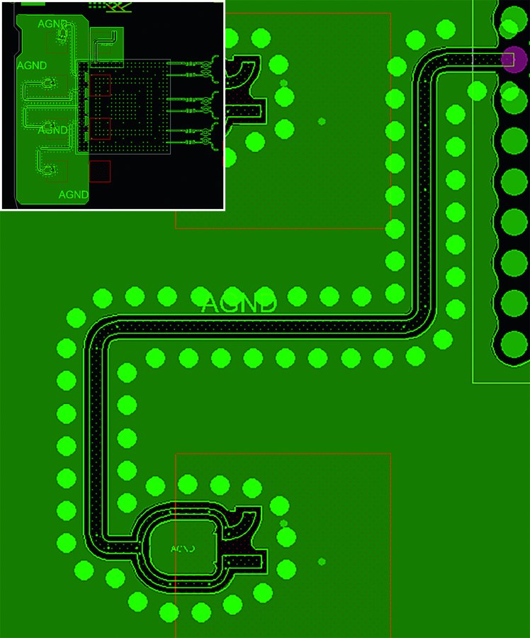
To protect the RF feed lines to the antennas from external interference, the lines can be shielded by ground planes with shielding vias. The distance between the vias and the shielding should be λ/6, i.e. one sixth of the wavelength used. After selecting the RF line, the pattern of the vias can be generated automatically. The shielding is taken into account during extraction and 3D simulation.
More interference from other devices
 Shielding of RF cablesWhenmore devices communicate via wireless interfaces, other devices can also be disturbed more. The increase in power densities and expansion of the frequency band therefore makes interference immunity to other devices even more important. Even developers who do not have RF applications on their PCBs must take into account that these can be disturbed by other devices from outside.
Antennas on PCBs are copper structures through which an alternating current flows, generating an electromagnetic field at certain frequencies. At the same time, the structures receive electromagnetic waves at the same frequencies and convert them into currents. This principle applies to all conductive structures on the PCB. EMC interference is nothing more than the unwanted reception of energy and conversion into currents that disrupt the behavior of the electrical circuit. As the number of wireless interfaces increases, so do the requirements for simulation and testing of EMC properties, in particular the interference immunity of all electronics.
