There are indications around the world that artificial intelligence (AI) is being used to raise the electronics industry to a new level of quality, either in part or as a whole. The most striking and at the same time most complex project is the DARPA project IDEA. While this is still a 'dream of the future', European, US and other companies are already offering practical ways of integrating AI into the electronics production process.
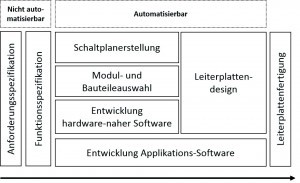 Fig. 1: Schematic electronics development process: many process steps can be mapped algorithmically and thus automated (Image: Contunity/Celus)Parts 1 and 2 of this report outlined the revolutionary goals of the rather monumental Darpa project IDEA/POSH. It is probably the most complex of the projects underway worldwide to use AI to take the development and production of electronics to a completely new level. The scope of IDEA is broad: it ranges from the efficient development of super ICs and complex semiconductor modules such as SoCs to the design and production of PCBs, assemblies and devices. To borrow a well-known popular expression, one could say that the project, which has been running since 2018, is aiming for a future 'egg-wool-milk-sow solution'. Whether, when and how it can or will be realized on this scale is not yet foreseeable. However, experience to date indicates that most steps in electronics development and production can be automated(Fig. 1). This will become even more important if we 'run out' of electronics developers in the near future. The number of electrical engineering students is declining and, according to publications, there will be a shortage of around 70,000 electrical engineers in Germany alone by 2026.
There are numerous examples in the electronics industry in the USA and Europe of AI already being used successfully on a much smaller scale than IDEA in the development and production of electronics. These are solutions that have been developed with incomparably fewer resources than IDEA and are constantly being developed further based on the experience gained. Examples of this can be found in Part 3 of this report. Figure 2 shows that the partial solutions range from circuit development and PCB design to the testing of PCBs, assemblies and devices.
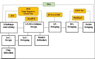 Fig. 2: Examples of the use of AI tools in the electronics development chain
Circuit development and PCB design with JITX
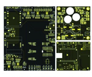 Fig. 4: Example of a board created with JITX Founded in 2017, Berkeley, California-based start-up JITX has spent the last three years developing an AI tool to automate PCB design, theoretically giving everyone access to professionally designed PCBs. The company is guided by the vision of automating hardware design for the benefit of science and humanity [1]. Ultimately, the aim is to automate the process of circuit and layout creation, which is increasingly becoming an unproductive bottleneck in the context of Industry 4.0 and interlinked smart factories, i.e. to adapt it to the high pace of forward development of electronic systems or to accelerate it significantly. This urgency comes at a time when AI is fundamentally changing the current state-of-the-art methods of the electronics industry. JITX is one of the companies connecting the new results of AI with the deepening problems in the market. Because the company is also a participant in the ERI and IDEA projects presented in Parts 1 and 2 of this article, it receives financial support from DARPA.
For IDEA, JITX is working with semiconductor and component manufacturers to build an extensive library of electronic components and develop software that turns high-level design targets into real circuit designs. Optimization tools are created to find the best possible version of the PCB. JITX is therefore helping to automate and streamline the entire process of developing electronic assemblies. In a further stage, the work will be extended from the electrical to the mechanical design, for example to housing development. This is in line with the objectives of ERI and IDEA at Darpa [2]. JITX is of the opinion that everything can be automated if the right approach is found and that the first partial results of IDEA should already be brought to market if they are practically usable, as in the case of the JITX tool of the same name. It can therefore be assumed that JITX is already a first result of the work on IDEA and POSH.
With the JITX tool, the still very young international team created a way to design electrical circuits and the PCBs based on them faster and with fewer errors than the service. Designs are generated with the help of codes. The basis is a general system block diagram and a description of the functionality. It needs a specification) in a DSL language that describes the components to be used and compiles them into KiCAD or Altium files. The latter can be sent to the PCB fab(Fig. 3, 4). In the development of JITX, methods of developing highly integrated circuits were adopted.
 Fig. 3: Example of the use of JITX DSL
The design files can also be output separately. The AI-supported solvers take care of the low-level details and make the engineering work reusable. A design in JITX is a code that captures the existing technical knowledge and makes it retrievable. There are no one-off circuit diagrams.
The user defines what is important to them, not how. For example, if a board with BLE (Bluetooth Low Energy) and a microphone (the 'what') is required, the software independently selects suitable key components from the library, designs power supplies and component values, obtains all parts, assigns pins, plans placements, routes the conductors and then exports the board and the circuit diagram (the 'how'). The tool exports a fully editable CAD project (KiCAD, Altium, etc.) as if it had been created by a human designer - only with better quality because the automated design process can rely on a constantly growing analyzed number of already realized designs.
If you have specifications for the shape of the PCB, constraints can be added as restrictions. The same applies to the position of components, the choice of certain BLE chips, etc. The authors believe that future design tools should be intelligent enough to solve the millions of details that the engineer doesn't care about. They should optimize the design towards what is important to the operator [2]. JITX can already be used practically by interested parties. A contact form can be filled out at [1]. At [3], interested parties can follow a discussion on Hackaday about the pros and cons of AI-supported design tools.
Circuit development and PCB design with Celus Supernova
![Abb. 5: Mit Hilfe der Automatisierung werden durch Celus Supernova nach Erfahrung der Fachleute die Entwicklungszeit und Time to Market um bis zu 90 % reduziert [5] Abb. 5: Mit Hilfe der Automatisierung werden durch Celus Supernova nach Erfahrung der Fachleute die Entwicklungszeit und Time to Market um bis zu 90 % reduziert [5]](/images/stories/Abo-2021-11/thumbnails/thumb_plus-2021-11-0076.jpg) Fig. 5: With the help of automation, Celus Supernova reduces development time and time to market by up to 90% in the experience of experts [5] The German company Celus (formerly Contunity) has developed Supernova, an AI cloud-based automation solution that reduces the complexity of electronics design with the help of an easy-to-use drag & drop tool [4]. It should be available in 2021. The start-up has set itself the goal of making electronics development processes faster, simpler and more efficient through automation. The all-in-one software solution enables the automated development of circuit diagrams and printed circuit boards as well as the creation of bills of materials (BOM). Pilot projects are currently being carried out together with various companies. Interested parties can contact the company if they would like to try out the tool. Celus has already received several awards: in 2018, the company won the Weconomy Award under its old company name Contunity, and in 2019 it received major funding as part of the EU's Horizon 2020 program.
Fig. 5: With the help of automation, Celus Supernova reduces development time and time to market by up to 90% in the experience of experts [5] The German company Celus (formerly Contunity) has developed Supernova, an AI cloud-based automation solution that reduces the complexity of electronics design with the help of an easy-to-use drag & drop tool [4]. It should be available in 2021. The start-up has set itself the goal of making electronics development processes faster, simpler and more efficient through automation. The all-in-one software solution enables the automated development of circuit diagrams and printed circuit boards as well as the creation of bills of materials (BOM). Pilot projects are currently being carried out together with various companies. Interested parties can contact the company if they would like to try out the tool. Celus has already received several awards: in 2018, the company won the Weconomy Award under its old company name Contunity, and in 2019 it received major funding as part of the EU's Horizon 2020 program.
According to [5], the engineers applied the principles of software development when developing Supernova and created the equivalent of a code generator. This is possible because the components can be selected solely on the basis of their tasks. The circuit diagram and layout can also be mapped using algorithms and artificial intelligence. In doing so, they took advantage of the trend towards developing sub-modules. The module data is stored precisely in a database so that proven sub-circuits, which may have already been certified, can be reused. In September 2018, the developers succeeded in developing the world's first functioning printed circuit board designed exclusively by algorithms. Supernova was developed to be fully integrated into the user's existing electronics engineering environment(Fig. 5).
Circuit development and PCB design with Circuit Tree
Under the motto 'Rapid Circuit Board Prototypes using Automation - Design and Order Boards in Minutes', the small Indian start-up Circuit Tree developed an automation engine that autonomously designs circuit diagrams and PCB designs with given user input via a GUI-based online tool(Fig. 6, 7). By using component definitions as proprietary models in its Octopart database, the company creates schematics, component placement and routing as a service in a very short time [6]. This means that the automation engine independently selects different types of components for a circuit and knows where these components need to be placed and routed on board. The Circuit Tree Design Engine was developed by engineers who have more than 20 years of experience in developing all types of first-time-right designs. However, after the automated development, the team checks the quality of the solution found again and thus continuously completes its database. It is estimated that the tool helps engineers to save between 70 and 90 % of the circuit design effort.
Circuit development with ACE
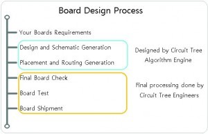 Fig. 6: Board design process at Circuit Tree Not quite as advanced as JITX and Celus in the use of AI is the London-based company Circuit Mind Ltd, founded in 2018. It is a start-up that supports companies in the development of electronic circuits from concept to prototype or through to production as a service, partly using AI. Its motto: Design reliable electronics in seconds. To fund its development work, Circuit Mind raised GBP 400,000 (approx. USD 550,000) from Deeptech Labs, a member of the Cambridge Network, in July 2021. Deeptech Labs is a start-up accelerator that was founded in Cambridge with the support of ARM, Cambridge Innovation Capital and the University of Cambridge [7]. In addition to small-scale financing, usually in return for 5 to 20 percent equity, the companies receive a three-month development program and access to mentors. These include some of the founders and managing directors of ARM, CSR and Imagination Technologies.
Circuit Mind's first product is the intelligent ACE platform, which uses AI to automatically select components and generate, optimize, maintain and redesign electronic circuit diagrams in a matter of seconds. The team is working to ensure that ACE will also be able to generate optimal PCB layouts with AI support in the future [8].
AI autorouter DeepPCB
In the simplest case, PCB layouts are still created manually by the designer, which can take a long time and be prone to errors. For more complicated circuits, automatic routing tools are used, which help to save an enormous amount of time. However, when converting the circuit diagram into a production layout, it is not always obvious which is the best routing strategy for a PCB, so that an optimum result for the assembly is not always achieved from a functional and cost perspective.
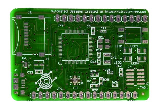 Fig. 7: Automatically created Micron Python board from Circuit Tree
Due to the varying quality of the autorouters on offer, the use of such a tool does not mean that the result cannot be significantly improved, especially when you consider that the biggest factor for good routing is still the best placement of the components. This is where AI increasingly comes into play, ideally drawing on a larger and better knowledge base.
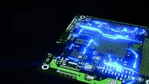 Fig. 8: Example of a board created with DeepPCB In 2019, the British company InstaDeep (headquartered in London) presented DeepPCB, the first AI-supported autorouter for printed circuit boards that customers can use as a service via a fully automated cloud platform [9]. TensorFlow-based machine learning is used. Partners in its development included Altium, Nvidia and Intel. InstaDeep also cooperated with various leading universities such as MIT, the University of Oxford and the University of Michigan. InstaDeep has built credibility in AI circles by innovating in the areas of Machine Learning (ML) and Reinforcement Learning (RL), especially in finding good solutions to NP-hard problems with AI.
The company was founded in 2014 and is now a leading company in the EMEA region for decision-relevant AI products [10]. It has offices in Paris, Tunis, Lagos, Dubai and Cape Town. Recently, InstaDeep was named one of the 100 most promising AI start-ups in the world by CB Insights for the second time in a row.
The DeepPCB platform works on the principle of 'no-human-in-the-loop' as soon as the user's .dsn PCB file has been submitted. The result is an SES file within 24 hours. Figure 8 shows a PCB created with DeepPCB.
The beta version of DeepPCB, which has been in use since 2019, relies on AI functions, which are constantly being expanded, and on proven hardware expertise. It was characterized by the following features in 2020:
- Routing for PCBs with up to 150 pairs and two layers (currently free to use)
- All routed boards are DRC (Design Rules Check)-tested and fully compatible with KiCad and Altium Designer
- Utilizing innovative InstaDeep AI technology in combination with powerful GPUs and cloud infrastructure.
Last year, the capabilities of DeepPCB were extended, e.g. to the routing of impedance-controlled PCBs. The EDA software preferred by customers can be used as before. Although the trend in electronics manufacturing is also moving towards the use of cloud services, it is possible that many companies do not want to entrust their designs to a cloud service, which slows down the learning process of the AI system and delays its practical usability. Interested parties can find a podcast with Karim Beguir from InstaDeep at [11], in which the expert spoke on the topic of Automating Electronic Circuit Design with Deep RL in April 2020. In [12], the company announced that it would also be addressing the use of AI in the component assembly of printed circuit boards as a key task from 2020.
The term DeepPCB is also used elsewhere in the literature, for example in the use of image analysis for error checking of boards based on 1500 published data sets or sample images of PCB cut-outs for research purposes [13]. Each of the sample images consists of a defect-free template image and an aligned tested image with annotations, including the locations of the six most common types of PCB defects such as open, short, etc. The 'DeepPCB trademark' was registered by the UK Intellectual Property Office (UKIPO) in 2019 with the 'application number' UK00003420198. The trademark application number is a unique ID to identify the 'DeepPCB trademark' in UKIPO.
AI in printed circuit board production at AT&S
The Austrian PCB manufacturer AT&S takes automated photos of the printed circuit boards during the manufacturing process. These are then run through image analysis software. According to Ulrike Klein, head of the Data & Analytics department at AT&S, it sometimes happens that PCBs are incorrectly recognized as 'faulty' - unfortunately without any comprehensible reasons. This costs the manufacturer additional time and resources.
In April 2021, AT&S announced that Know-Center GmbH had developed an AI algorithm for the company that should significantly improve the situation. The algorithm not only correctly recognizes the images of the PCBs, but also provides an additional explanation as to why a PCB has been identified as defective or intact. This means that AT&S now has a transparent AI system at its disposal which, following an intensive test phase, should deliver comprehensible and explainable results in the foreseeable future [14].
The Graz Know-Center GmbH (full name: Research Center for Data-Driven Business & Big Data Analytics) is one of the leading European research centers for Data-Driven Business and Artificial Intelligence (DDAI). As an outsourced research institution of Graz University of Technology (also majority shareholder) and center of excellence in the COMET program, it has been conducting basic research since 2001 and is internationally networked with numerous EU projects, including the EU Horizon 2020 program. The research GmbH currently has 130 employees from 20 countries [15]. COMET, in turn, is a network of 25 institutions in Austria that is funded by the government. The existing scientific and technological expertise is pooled in the nationwide COMET centers, thereby sustainably strengthening Austria's competitiveness as a research location. The network currently consists of 22 COMET projects, 25 COMET centers and 6 COMET modules. The algorithm for AT&S mentioned above was specifically developed by the DDAI module of Know-Center GmbH [16]. AT&S is one of the industrial partners in the COMET module DDAI. In the future, further projects in the direction of 'Trustworthy AI' are to be driven forward together with AT&S and other industrial partners of the module.
Integration of AI in optical inspection systems for component and device production
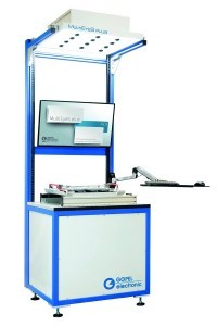 Fig. 9: AI-supported smart automatic optical inspection module MultiEyeS plus from Göpel electronic for integration into assembly and THT assembly stationsDespitethe increasing automation of assembly processes in the production of electronic assemblies, many assembly processes will still be carried out manually in the foreseeable future, for example when assembling printed circuit boards with THT components. As humans are involved here with their liability for errors, the question arises as to how the quality of the corresponding production process can be better monitored in such cases. The Jena-based company Göpel electronic is taking this approach by directly integrating optical inspection systems into assembly and placement stations, combined with automatic logging. According to the author of the article in [17], the direct integration of optical inspection into the assembly process requires completely new and original device concepts compared to traditional AOI systems. The cameras for inspection must be arranged in such a way that they do not interfere with the assembly process of the people working there. The lighting cannot be optimized for the requirements of image processing, but must meet the legal requirements of a workplace for assembly processes. In addition, light-shielding cladding is not possible, as this would restrict the manual assembly process.
With MultiEyeS plus, Göpel electronic has developed a self-learning inspection module that is ideally suited to such processes and has an image area of 550 x 450 mm [18]. The system is based on multi-camera image acquisition technology, an image acquisition unit consisting of up to 12 cameras with integrated lighting, in which the individual images are then combined into a single image using a stitching algorithm. Although the open system used here is not optimal from the point of view of classic image processing, the powerful software is coupled with an AI-based solution. More on this can be found in [17] and [18]. According to Göpel, the principle used enables images to be captured with outstanding image quality and very high detail resolution. Based on the PILOT AOI system software, an inspection speed of up to 800 cm²/s is achieved.
The combination of classic image processing technology with powerful AI functions creates a system that works reliably even without light shielding and offers the possibility of further optimizing the assembly of THT components, for example(Fig. 9). Another field of application would be the assembly of components in housings.
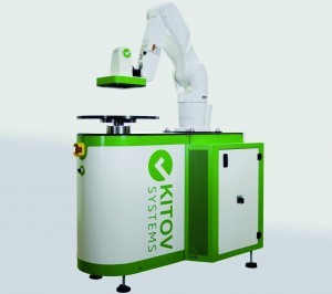
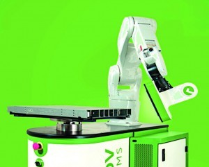
A smart AI-supported AVI system for checking the final quality of assemblies and end products, which can probably be used even more widely in quality control than Göbel's MultiEyeS plus, was already mentioned in Plus 6/2021 [19]. KITOV One is the first smart 3D hybrid universal system that can effectively inspect virtually any product, regardless of the industry. By using 3D computer vision algorithms and artificial intelligence based on machine learning and deep learning, an extremely high level of recognition is achieved. The AVI system from the Israeli company Kiton supports complex 3D structures, numerous materials and complete inspection specifications. The universality of the system's application results not least from the combination with a 6-axis robot unit of the Scara type and a rotary table(Fig. 10). The system scans products up to a size of 850 x 420 mm. More information on the application in the area of Highly Variable Electronic Product Mix can be found in a white paper [20].
In Figure 11, the inspection system is used for the final inspection of finished electronic modules. It can be used to detect cosmetic defects such as scratches, dents, differences in color, smeared labels, human hair strands or fingerprints, but also bent pins on ports and connections, screws that have not been tightened, missing components or incorrect barcodes. When considering the cost of such an inspection system, it is worth remembering that any faulty product that is packaged and shipped as a finished good or integrated into a complex system may well become a painful cost issue and damage brand reputation and customer satisfaction.
A case study on the use of KITOV One to control high-end switches at an IT manufacturer is briefly presented in [21]. A simple but frequently found error was, for example, an incorrectly placed label(Fig. 12).
The economic result of the case study: an ROI (return on investment) of just six months. However, this should not obscure the fact that it takes considerable effort on the part of the device manufacturer to 'teach' the system.
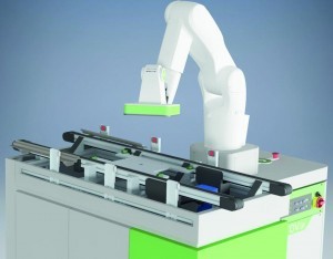
Figure 13 symbolically demonstrates the integration of KITOV One into a production line, as can be the case in both PCB and assembly production.
Ongoing AI research projects for the electronics industry in Germany
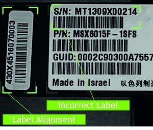 Fig. 12: A poorly placed label - not a functional defect, but also not proof of careful workToconclude this article, we should take a look at research in Germany. About three years later than in the USA, a major research project for AI-supported development methods for large electronic systems was also launched here with the progressivKI funding project. Not only is it nowhere near the scope of IDEA/POSH or even ERI and is purely civilian in nature, it is primarily aimed at the automotive industry.
The project runs from April 1, 2021 to March 31, 2024 [22]. Funding reference number: 19A21006A-R. The progressivKI project has a long project title: Supporting the development of efficient and safe electronic systems for future automotive applications with automated driving functions using a modularly structured AI platform. The aim of the project is to develop a generalized AI-supported design process for automotive electronic systems. The use of AI methods in the respective design processes is intended to accelerate system development and at the same time improve the validation of the functional safety of electronic vehicle components. A modular AI platform is being developed that can be used flexibly via secure, encrypted and intelligent connectors to the individual (distributed) modules and subsystems. A link with GAIA-X is also realized via these connectors. AI-supported feedback and integrated domain-specific knowledge are intended to support electronics developers in the design of complex systems and thus make the entire design process more efficient. In addition, progressivKI will develop procedures to evaluate and validate the quality of the training and learning processes of the implemented AI methods. The developed system is to be implemented as a prototype and applied and demonstrated using two applications (PCB and IC design, intelligent sensor technology).
The project involves 18 project partners and four other research partners. The project is coordinated by Robert Bosch Car Multimedia GmbH and project managed by edacentrum GmbH and Pyramide2525. Edacentrum is a German-based network for electronics, design and applications in business and science. The BMWi is contributing €11.2 million in funding. The project participants include universities and colleges, Fraunhofer Institutes, large companies and SMEs such as Binder Elektronik.
Zuken joined the project as one of the industrial partners with its EMC Technology Center development site in Paderborn [23]. Ralf Brüning, Product Manager and Senior Consultant at the Center, has taken over the management of the work package, which includes the basic definition of requirements and specifications, in addition to helping with the industrial coordination of the project. With its participation, Zuken intends to contribute its expertise in the analysis (signal and power integrity) of PCB structures to the project in order to realize a connection to the AI modules and thus support the learning/training process in the planned cooperation with the various partners in the consortium. The company also wants to significantly improve the Zuken 'PCB Design Software' and analysis functionalities. Dr.-Ing. Werner John from edacentrum assessed the project as follows: "The progressivKI project has the potential to become a beacon in the implementation of AI-supported methods in the EDA area and to stir up future-oriented industry-driven implementations [23].
Compared to other AI-supported service offerings mentioned in this multi-part article, doubts may arise as to whether progressivKI was not initiated a little late and whether the focus of the funding project is not somewhat one-sided, especially with regard to the interests of car manufacturers.
References:
[1] www.jitx.com
[2] https://spectrum.ieee.org/startup-jitx-uses-ai-to-automate-complex-circuit-board-design
[3] https://hackaday.com/2018/10/16/cool-tools-deus-ex-autorouter/
[4] www.celus.io/en/product-supernova_new
[5] www.gategarching.com/gateway_story/gatepeople-contunity-gmbh/
[6] https://circuit-tree.com/
[7] https://cambridgenetwork.co.uk/directories/companies/172494
[8] www.circuitmind.io
[9] https://deeppcb.ai/
[10] www.instadeep.com/
[11] https://twimlai.com/twiml-talk-365-automating-electronic-circuit-design-with-deep-rl-w-karim-beguir/
[12] https://deeppcb.ai/faqs
[13] https://github.com/tangsanli5201/DeepPCB
[14] www.ats.net.at
[15] www.know-center.tugraz.at
[16] https://ddai.know-center.at/
[17] Plus 8/2021, p. 1023ff
[18] www.goepel.com/inspektionsloesungen/aoi/tht-inspektion/multi-eyes-plus.htm
[19] Plus 6/2021, p. 714-715
[20] www.kitov.ai/wp-content/uploads/2021/06/Kitov_USTech_v2.pdf
[21] www.kitov.ai/solutions/high-end-electronics/
[22] www.edacentrum.de/projekte/progressivKI
[23] www.zuken.com


