Sustainability plays an important role in the development and manufacture of innovative products. Innovation not only means faster, better, cheaper, but also more energy-efficient and environmentally friendly - and also enables more efficient recycling. In the EU-funded ReIn-E project, the INM - Leibniz Institute for New Materials is working on this topic together with project partners.
Modern electronics applications require ever greater miniaturization. This applies not only to the electronics themselves, but also to their combination with the materials that hold and protect them. Conventional components are often too bulky and inflexible. It is therefore not surprising that the industry is increasingly turning to space-saving solutions. The idea of integrating electronic elements directly into a carrier material or printing them onto it is an obvious one. So-called in-mold and printed electronics technologies are economical, enable new designs and save space, weight and material.
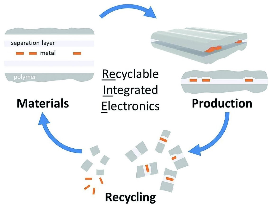
 Components and plastic carriers can be separated at the end of a product's life thanks to an intermediate layer that can be split up again in the recycling process
These would be ideal conditions for their use in vehicles or household appliances if it weren't for one serious disadvantage: at the end of the product's life, it will be very difficult to remove the electronics from the appliances and recover the raw materials by type. Even with conventional metal-plastic components, material separation and subsequent recycling are difficult; with polymer-integrated electronics, this is almost impossible
This is where the ReIn-E project comes in, which entered its second half in January 2022: the aim of the project is to develop recycling-friendly designs and sustainable materials to enable the components to be recycled. At the INM in Saarbrücken, Prof. Tobias Kraus and his team are researching a layer that is applied between the polymer and metal. This separating layer must be designed in such a way that it ensures optimum adhesion of the two components during use of the component and enables the plastic and metal to be separated again if necessary.
Kraus explains the research approach: "A solution of water and polyvinyl alcohol (PVA) is applied to the surface of a polymer substrate into which current-conducting materials are to be integrated. PVA is a water-soluble plastic and behaves in a similar way to table salt: it dissolves in the liquid and can be returned to its original solid state by heating and evaporating the water. By adding water again, the PVA film becomes liquid again. In this way, the different materials of in-mold and printed electronics can first be connected via the PVA layer and then separated again. If the components are no longer used, their components can be recycled separately."
In addition to the development of the separating layer, the INM is dedicated to the synthesis of special pastes and inks for printing electronic circuits, thus complementing the project tasks of the partners from Belgium and Germany: The Centre Terre et Pierre specializes in recycling processes for solid waste and electronic scrap and develops processes for the recovery of metals and polymers, the Hahn-Schickard-Gesellschaft für angewandte Forschung prints electronics and tests the performance and stability of the printed and integrated materials and structures, and finally, the Sirris Technology Research Centre will manufacture the integrated components based on the developed designs and materials.
A special feature of the ReIn-E project is the involvement of small and medium-sized enterprises (SMEs), which could play a key role in the sustainable transformation of electronics manufacturing. The aim is to enable them to help shape and benefit from the transition from conventional technology to integrated electronics.
About the INM
The guiding principle 'New materials are the driving force behind new technologies' describes the fundamental approach of the INM. The Saarbrücken-based institute of the Leibniz Association combines multidisciplinary science and material-oriented technology transfer under one roof. Chemistry, physics, biology, materials science and engineering work together in close cooperation. A key focus of the research work is the transfer of biological principles to the design of new materials, structures and surfaces. The INM is networked worldwide with numerous research organizations and technology companies.
Contact person:
Prof. Dr. Tobias Kraus, INM, Head of Program Area Structure Formation, Tel.: 0681 9300 389, Mail:
Dr. Mariano Laguna Moreno, INM, Head of Structural Engineering, Tel.: 0681 9300 370 Mail:


