
The production of thick aluminum layers at moderate temperatures is of great interest for many areas of application. This article examines the electrodeposition of aluminum for printed circuit board and microsystem technology. Influencing variables on the layer morphology are presented on the basis of depositions on silicon substrates with a gold starting layer. The current density and the electrolyte temperature have a major influence on the microstructure of the layers produced. The deposition parameters evaluated for the gold starting layer cannot be transferred to an aluminum starting layer.
The production of thick Al layers at moderate temperatures is of great interest for many applications. In this paper the galvanic deposition of aluminum for printed circuit board and microsystem technology is investigated. Influencing variables on the layer morphology are represented by deposition on silicon substrates with a gold seed layer. The current density and the electrolyte temperature have a great influence on the microstructure of the layers produced. The deposition parameters evaluated for the gold seed layer cannot be transferred to an aluminum seed layer.
Vias are very important for a functional printed circuit board. In this article different approaches for the coating of such through-hole contacts are presented. Furthermore, the structuring of the aluminum layers is described using photoresist including etching of the seed layer.
Through-hole contacts are very important for a functional printed circuit board. Various approaches for coating such through-contacts are presented in the article. Furthermore, the structuring of the aluminum layers using photoresist including etching of the seed layer is described.
4.1.2 Influence of temperature and current density on the layer morphology
 Fig. 5: SEM images for IL temperatures of 30 °C and 50 °C for three different current densities: 5 mA/cm2, 13 mA/cm2, 26 mA/cm2Theelectrical conductivity and viscosity properties of the IL are influenced by the temperature: the electrical conductivity increases and the viscosity decreases. The extent to which this temperature dependence also influences the layer morphology is shown below. The parameters are as follows:
- 3 Current densities: 5 mA/cm2, 13 mA/cm2, 26 mA/cm2
- 4 Temperatures: 30 °C, 40 °C, 50 °C, 55 °C
- Floating charge approximately constant, so that approx. 1 µm layers are deposited
Figure 5 illustrates the influence of increasing current density at constant temperature on the microstructure. SEM images for all three current densities and two temperatures (30 °C and 50 °C) are shown. It is clear that the layers become more finely crystalline as the current density increases. This effect can also be seen at 40 °C and 55 °C.
It is also clear that the microstructure for 5 mA/cm2 and 13 mA/cm2 becomes coarser as the temperature increases. In contrast, the 26 mA/cm2 layer remains optically the same. This influence continues at an IL temperature of 55 °C, so that the layer deposited at 26 mA/cm2 remains optically unchanged. The optical appearance can be confirmed by means of white light interferometric (WLI) roughness measurement (see Fig. 6). The roughness for 26 mA/cm2 is below 10 nm in an area of 100 × 100 µm2 at all temperatures. The increase in roughness at lower current densities can be explained by a faster surface diffusion of the Al atoms to form crystal nuclei. This results in larger crystallites instead of new crystal nuclei. At higher current densities, on the other hand, the crystallization overvoltage, i.e. the compulsion to form new nuclei, is so high that the layers hardly change when the temperature is increased. The potential-time curves for the respective current densities show that the deposition potential decreases with increasing temperature. At j = 13 mA/cm2 the potentialdrops from approx. 0.8 V (30 °C) to approx. 0.55 V (55 °C). For j = 26 mA/cm2, the potential is reduced from approx. 1.6 V (30 °C) to approx. 1.05 V (55 °C). As the layers for the two current densities at 30 °C differ only minimally, it can be assumed that a deposition potential > 800 mV is required to obtain fine crystalline layers.
 Fig. 6: Dependence of the RMS roughness of the Al layers on the IL temperature for three current densities
The current yield increases with temperature at j = 26 mA/cm2. At 30 °C, the current efficiency is approx. 80 %. At 50 °C, however, it is already approx. 93 %. At the lower current densities, the current yield deteriorates with increasing temperature.
The following conclusions can be drawn:
- Depositions at almost room temperature (30 °C) can be carried out equivalently with j = 13 mA/cm2 and j = 26 mA/cm2.
- Depositions at higher temperatures (50-55 °C) should be carried out with higher current densities (j = 26 mA/cm2).
- The deposition potential should be greater than 800 mV in order to obtain fine crystalline layers.
4.1.3 Influence of the current flow
 Fig. 7: SEM images of the Al layers for 30 °C and 50 °C at jpeak = 26 mA/cm2 From chapter 4.1.2 it is clear that higher current densities have a positive effect on the layer morphology. It is known from the literature that pulsed current deposition leads to fine crystalline and dense layers [14]. As there are hardly any studies [15, 16] on pulse current deposition from the EMImCl/AlCl3-IL, selected parameters are compared below.
The peak current density jpeak is set at 26 mA/cm2 for the investigations. The frequency f (10 Hz or 50 Hz), the duty cycle dc (90 % or 50 %) and the temperature (30 °C or 50 °C) are varied. Only unipolar pulsing is considered in this comparison.
The microstructures are shown in the SEM images in Figure 7. The images are arranged according to temperature and average current density, frequency and duty cycle. These SEM images are also shown for better comparability with DC deposition.
|
Current yield |
Separation rate |
Current efficiency |
Separation rate |
|
|
DC |
80 % |
230 nm/min |
92 % |
264 nm/min |
|
PP 10 Hz, 90 % |
75 % |
328 nm/min |
94 % |
413 nm/min |
|
PP 50 Hz, 50 % |
139 % |
188 nm/min |
163 % |
220 nm/min |
It can be seen that the microstructures at TIL = 30 °C hardly differ from each other. At TIL = 50 °C, however, a large difference between the pulse current parameters can be seen. The decisive parameter is the duty cycle, as similar behavior is also observed at f = 10 Hz and dc = 50 %. Due to the lower duty cycle, the average current density decreases, whereby the deposition process behaves analogously to direct current deposition. The comparison of the SEM images of the pulse current parameters f = 10 Hz, dc = 90 % with the direct current deposition shows hardly any difference.
The process parameters current efficiency (CE) and deposition rate are decisive for a reliable process. Table 1 lists these characteristic values for the parameters used here. It is clear that the process parameters for all separation parameters increase at TIL = 50 °C. Since the ion concentration upstream of the cathode reaches a quasi-steady state in pulsed current deposition, which is higher than in direct current deposition, it is possible to increase the deposition rate [17]. This means that less time is required to achieve a target layer thickness with the pulsed current method.
The current yield of the sample with f = 50 Hz, dc = 50 % can be explained by a measurement error.
4.1.4 Influence of the starting layer on layer formation
 Al-Startschicht, jpeak = 20 mA/cm2; B) Al-Startschicht, jpeak = 10 mA/cm2; C) Au-Startschicht, jpeak = 20 mA/cm2") Fig. 8: SEM images of the electrodeposited Al layers for Al and Au starting layers at f = 25 Hz and dc = 90 %. A) Al starting layer, jpeak = 20 mA/cm2; B) Al starting layer, jpeak = 10 mA/cm2; C) Au starting layer, jpeak = 20 mA/cm2Aland Au exhibit very different behavior as starting layer materials. Al oxidizes immediately on contact with air. Au does not react with air and is therefore an ideal starting layer. The analysis of the influence of the starting layer is carried out using structured deposits at wafer level. The structure widths are 80 µm (Au) and 60 µm (Al). The structure widths in these sizes have no influence on the layer formation.
Fig. 8: SEM images of the electrodeposited Al layers for Al and Au starting layers at f = 25 Hz and dc = 90 %. A) Al starting layer, jpeak = 20 mA/cm2; B) Al starting layer, jpeak = 10 mA/cm2; C) Au starting layer, jpeak = 20 mA/cm2Aland Au exhibit very different behavior as starting layer materials. Al oxidizes immediately on contact with air. Au does not react with air and is therefore an ideal starting layer. The analysis of the influence of the starting layer is carried out using structured deposits at wafer level. The structure widths are 80 µm (Au) and 60 µm (Al). The structure widths in these sizes have no influence on the layer formation.
For deposition on Al, a 2-minute anodic reverse pulse is switched at a low current density. The current density (jpeak = 10 mA/cm2 or 20 mA/cm2) is then varied by means of pulse current deposition. The frequency and the duty cycle are constant at 25 Hz and 90 %. For the Au starting layer, jpeak = 20 mA/cm2 and the same frequency and duty cycle are used. Figure 8 shows the generated layers at different positions on the wafer. Rows A and B represent the Al starting layer at 20 mA/cm2 and 10 mA/cm2 respectively. For A, a layer thickness of 20 µm was targeted. Ultimately, the layer is only a few 100 nm thick. As a result, the current density for B and the target layer thickness were reduced. It is noticeable that the current density behavior of the Al starting layer does not correspond to the results known from chapter 4.1.2. According to this investigation, deposition on the Al starting layer with lower current densities is more effective. Nevertheless, the coating of sample B is also unsatisfactory. The edges of the structure are too high and the layers are often not closed at the edge of the wafer. To check whether this is a layout or starting layer effect, the depositions with Au starting layer (row C) were repeated. The dark triangular particles at the edges of the structure are paint residues that have not been properly removed. For jpeak = 20 mA/cm2 and a targeted layer thickness of 5 µm, a homogeneous, even layer corresponding to the target thickness is achieved. Consequently, the layout has no influence on the basic deposition. The influence of the starting layers can be impressively demonstrated.
The results show that the galvanic deposition of Al on an Al starting layer is not trivial. The use of a zincate and nickel process should be avoided in order to ensure a homogeneous material system. Another approach to successful coating of the Al starting layer is a step-like adjustment of the current. The extent to which it makes sense to start with high or low current densities is currently being investigated.
4.2 Printed circuit board substrates
Al deposition on Cu-laminated PCBs behaves in a similar way to that on an Au starting layer. The greatest challenge here is the coating of vias. Different pre-coatings of the vias in the test substrates were used for this purpose:
- Intrinsically electrically conductive polymer
- Black hole (graphite pre-coating)
- Copper stop
The substrates were provided by Jenaer Leiterplatten GmbH.
4.2.2 Conductive polymer
 Fig. 9: SEM image of the cross-section of a 200 µm via: Deposition parameters: TIL = 30 °C, direct current deposition: j = 40 mA/cm2, t = 900 sThe aimis to work as closely as possible to the existing production process in PCB technology. Electrically conductive polymers are a common via pre-coating to achieve a basic conductivity of the vias so that the vias can subsequently be electroplated with Cu. However, the conductivity of the polymer is greatly reduced within a few days due to oxidation processes, so that further processing must be carried out quickly after the delivery arrives.
A sample with an Al penetration depth of approx. 70 µm into the via is shown in Figure 9 as a representative of the series of tests with electrically conductive polymer. The current density of j = 40 mA/cm2 is relatively high, although no Al coating could be traced in the vias with lower current densities. Further work with the polymer-filled vias proved to be unsuccessful. Due to the above-mentioned decrease in conductivity during exposure to air, the production of Al-coated vias has not yet been possible. As a result, the long-term stable graphite coating has been used.
4.2.2 Black hole (graphite pre-coating)
Coating with direct current is also not promising for graphite coating in the vias. The subsequent pulsed current depositions show more promising results. The pulse parameters are selected according to the results on the Si substrates: jpeak = 26 mA/cm2, f = 10 Hz, dc = 90 %.
Based on the cross-section analyses(Fig. 10), a penetration depth of the Al of approx. 550 µm for a 600 µm via can be specified for these parameters. Furthermore, the Al layer thickness in the via is sufficiently high at approx. 27 µm. However, the layer thickness on the surface is considerably lower. The penetration depth on the opposite side is very low at approx. 90 µm. This could be explained by a slight tilting of the electrodes, so that the effective current density was lower at this point. Other samples with the same parameters show similar coating behavior.
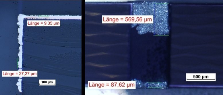 Fig. 10: Light microscope image of the cross-section of sample Bh10 (a 600 µm via is shown)
The conclusion of the experiments is that Al coating of vias with the Black Hole precoating is certainly possible. However, it remains to be clarified whether the flow through the vias is sufficiently high to ensure a complete coating.
-to be continued-
