Not only the tabloids, but also the serious German media go into overdrive when - as in London, for example, two Habsburg descendants - 'blue-blooded' people say yes to each other. Not all journalists [2] seem to have realized that the aristocracy in Germany no longer has any special rights since the Weimar Republic [3]. Nevertheless, thanks to the Brothers Grimm [4], we all know how the 'blue-bloodedness' - i.e. 'authenticity' - of a princess can be proven by means of a pea.
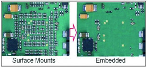 Fig. 2: An assembly reworked from SM to embedded technologyThemany mattresses and the pea are strongly reminiscent of a multilayer board with embedded components. So when we talk about a mattress bed in electronics, we are not thinking of the thin-blooded nobility but of printed circuit boards, which hopefully do not conceal a dry, uncooked pea.
Embedded components are currently in vogue because they have a number of advantages, although some difficulties should not be concealed. The attempt to embed components in the PCB is not entirely new [5]. However, we have come a long way from the rather 'primitive' beginnings of inserting resistors into vias, and what you can find inside certain PCBs today goes well beyond passive components.
Whenever a new technology makes its presence felt, it is driven by a number of advantages that are either realistic or just clever marketing. Obvious advantages are cited:
- A potential reduction in the size of the assembly, as fewer components are arranged on the surface
- Or, in the case of cell phones for example, the number of components can be increased and the functionality expanded without having to change the size.
- The shortening of the conductor paths reduces self-induction and thus allows a higher speed of the circuit.
- Interference is reduced by locking the components in a Faraday cage.
- Although the cost of the PCB increases, the overall cost of the assembly may be lower.
- Thermal problems can be better managed by making good use of PCB properties (such as aluminum).
- Some reliability problems are reduced, as internal components are less sensitive to PCB bending than those mounted on the surface.
The biggest disadvantage is currently seen as the lack of training among engineers who have no experience in layout or production. In addition, most of the computer programs used have not yet integrated this technology, leaving the engineer alone when it comes to tolerances and other critical specifications. The problem is understandable to a certain extent, as almost every company has introduced a different procedure that is specifically tailored to their product.
 Fig. 3: Example of a PCB with active and passive embedded components (1 = core with two-sided copper coating; 2 = base for component placement; 3 = prepreg with cut-outs for components; 4 = copper-coated dielectric)
It must be clear to the process engineer that repair is largely impossible, which can be a real and possibly expensive obstacle, especially with active components inside.
Two cases are given here as examples of the procedure for manufacturing such printed circuit boards.
A thin prepreg and a copper foil are placedon a pre-laminated substrate (Fig. 4), which consists of a structured FR4 core and already contains a cut-out for the Schottky diode. This stack is pre-laminated onto a substrate. During the subsequent lamination, the prepreg layer only acts as an 'adhesive layer' as it has not been fully cured. The silicon chip is now sunk into this substrate. The predetermined recesses in the FR4 core determine the position of the chip and must be arranged as precisely as possible.
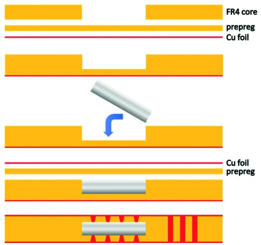 Fig. 4: Process sequence for double-sided Cu micro vias
Additional layers are then built up (prepegs plus copper foils). Lamination takes place in a standard multilayer press. This procedure creates a completely symmetrical structure that centers the chips in the middle of the core.
The electrical contacts on the anode and cathode of the embedded chip are created using microvias. To do this, holes are drilled with a UV laser. The connection of the anodes from the front to the back of the circuit board requires the mechanical drilling of holes for through-hole plating. The copper metallization of the vias is then created. Lithography and structuring etching form the final step.
By no means all components that you would like to sink into the inside of the PCB are immediately suitable for this. Since most are coated with aluminum for conventional gold wire bonding, but the connections in the PCB use different chemistry and techniques, intermediate steps must be taken to prepare the component for use (see Fig. 5for examples of possible connection configurations ).
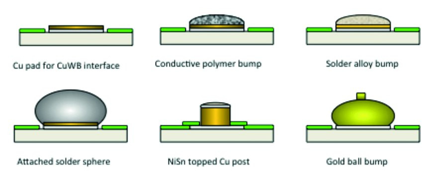 Fig. 5: Connection surfaces modified depending on the subsequent connection technology (STC)
Another of the many variants of the process sequence was developed by HERMES, a consortium of industry and academic institutes. This uses a combination of HDI production and micro ablation and plating as well as a semi-additive coating technology for ultra-fine lines. The approach is suitable for both discrete passive and active components.
First, reference marks are marked on the surface of an ultra-thin copper foil base layer using a laser. Adhesive is applied to the copper surface and partially cured. The components are then placed in the adhesive pattern so that the connection surfaces face downwards. A thermal curing process follows.
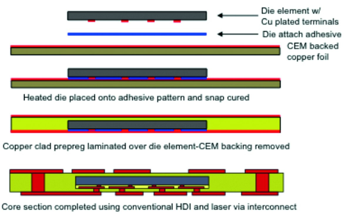 Fig. 6: Variation of a theme (AT&S)
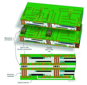 Fig. 7: Solderless aluminum substrates with internal components can even be stacked and 'riveted' togetherThenadditional pre-punched or laser-ablated FR-4 prepregs are applied. Finally, everything is laminated using a conventional multi-layer vacuum press. The PCB is then more or less finished using standard methods (see Fig. 6).
A particularly promising method for certain technologies - also a variation on the theme of embedding - uses aluminum substrates and does not require soldering(Fig. 8).
Under the generic term SAFE (the acronym stands for either 'solderless assembly for electronics'or 'solder alloy free electronics'), the electrically tested components are mounted on an aluminum substrate and the connections are made using copper.
Again, a long list of benefits are mentioned, ranging from cost savings to environmental friendliness, with some of the electrical, electronic and thermal ones certainly being the most interesting.
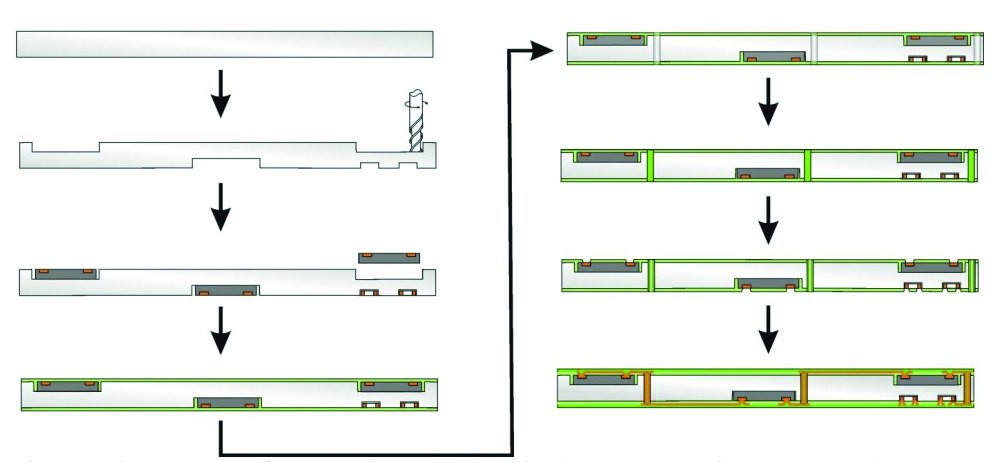 Fig. 8: Process steps for a double-sided aluminum circuit assembled without solder
Literature and notes:
G. Mayr: Embedded Components: A Comparative Analysis of Reliability Part II, IPC APEX EXPO Conference Proceedings
J.S. Peiffer: Embedded Passives Become Mainstream Technology, Finally!, IPC APEX EXPO Proceedings
H. Chammas: Embedded Passive Technology, IPC APEX EXPO Proceedings
V. Solberg: Embedding Passive and Active Components: PCB Design and Fabrication Process Variations, IPC APEX EXPO Conference Proceedings
IPC-7092: Design and Assembly Process Implementation for Embedded Passive and Active Components, Standard publication, IPC.org
S. Johansson et al: Miniaturization of Hearing Aid Electronics using Embedded Die Packaging, SMTA Proceedings
J. Fjelstad; Method for the Manufacture of an Aluminum Substrate PCB and its Advantages; IPC proceedings
References:
[1] Spanish 'Sangre azul' - Under Moorish rule in Spain (711-1492), the term 'azure blood' was applied to the upper class descended from the Germanic Visigoths
[2] https://www1.wdr.de/stichtag/stichtag1170.html
[3] https://de.wikipedia.org/wiki/Deutscher_Adel#Nachfolgeorganisationen_des_deutschen_Adels
[4] Actually already in Hans Christian Andersen
[5] US3519959A: Integral electrical power distribution network and component mounting plane; 1966
[6] HERMES - High density integration by Embedding chips for Reduced size Modules and Electronic Systems. The Hermes partners are ASM Assembly Systems, Atotechm, Bosch, Circuit Foil Luxembourg, Fraunhofer IZM, Fundico, IMEC, Infineon, Roodmicrotec and Thales Communications & Thales Corporate Services

![Blue blood[1]](/images/k2/ae623343d9b0e22dc5d6db49e92f6c40.jpg)
