Thanks to the now fully operational 'Research Fab Microelectronics Germany' (FMD) and the twelve upstream chip technology research laboratories (Forlabs), Germany has now created a virtual large-scale microelectronics research center that can compete with Imec in Belgium and Cea-Leti in France - as FMD director Prof. Albert Heuberger puts it: "This means we can now play better on the European playing field - also within the framework of the EU Chips Act." There are high hopes for this in Saxony.
Heuberger, who also heads the Fraunhofer Institute for Integrated Circuits (IIS) in Erlangen and the FMD Steering Committee, is not alone in his assessment at the digital conference 'Microelectronics Research in Germany: From Fundamentals to Applications' in Dresden. This Chips Act, through which EU Commission President Ursula von der Leyen wants to activate around €43 billion in public and state funding for Europe's semiconductor industry, is giving representatives from business and politics in Saxony high hopes of a new boost for their microelectronics industry.
 The chain from the computer model to the electrically functionalized injection-moulded part to the finished component with electrical connection: In this specific example, magnetic field sensors were also integrated into a gear cap
Dresden cabinet stakes out claims in Brussels
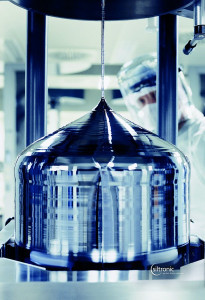 Siltronic manufactures wafers for the large chip factories from such silicon growing crystals, called ingots. The company is now investing millions more in the Freiberg site In order to stake its regional claim, the Saxon cabinet moved its meeting from Dresden to Brussels on May 10 without further ado. The aim was to fly the flag there and once again draw the attention of decision-makers at EU level to the particular importance of the semiconductor industry. "The European Chips Act is enormously important for Europe and Germany in order to become more independent in the key microelectronics sector," emphasized Minister President Michael Kretschmer. "The global political situation requires us to act quickly," he said, referring to dependencies and disrupted supply chains as a result of the coronavirus pandemic and the war in Ukraine. "Bavaria is doing everything it can to ensure that Europe's chip offensive is a success. The project is important for our continent and at the same time a huge opportunity for Saxony to further consolidate its position as a leading European microelectronics location."
With the FMD, players from Saxony and the whole of Germany have already created a virtual fab in recent years, which at least partially brings together semiconductor research activities that were previously widely dispersed. It was primarily at the urging of the Fraunhofer-Gesellschaft and the Saxon microelectronics industry that the then Federal Research Minister Johanna Wanka pledged around €350 million in 2017 to set up the virtual network of pilot lines, which are working on a wide range of microelectronics development projects across Germany. A dozen Fraunhofer and two Leibniz institutes were and are involved. An office in Berlin was responsible for coordination.
In total, the participating FMD institutes had used the funding to procure around 250 new systems by the end of 2021 in order to close gaps in their scientific and technical chains. One investment focus was on the semiconductor research cleanrooms in Dresden. Now that the set-up phase has been completed, the FMD will largely finance itself through industrial contracts.
Forelabs docked to the research factory as a university preliminary stage
From 2019, twelve Forelabs, which focus more on preliminary research, were docked onto this FMD for pilot production. They received around €50 million to close their hardware gaps. The 14 participating universities ordered a total of 100 systems, 96 of which have now been delivered. "There were some delays due to coronavirus and Brexit, which is why we have extended the project slightly," reported Forlab coordinator Prof. Thomas Mikolajick from TU Dresden. However, the last systems should be delivered by November 2022. This means that "university locations throughout Germany have excellent equipment and infrastructure," he emphasized. "This can and must be used intensively." He called for the Forlabs to be opened up more to spin-off high-tech companies in future, so that they can rent clean rooms, for example.
Mikolajick also sees better opportunities thanks to networking through the FMD and the Forlab network: "This has created a considerable 'innovation funnel'. This refers to the very broad preliminary research in the Forlabs, which is later funneled into a selection of pilot lines in the FMD institutes.
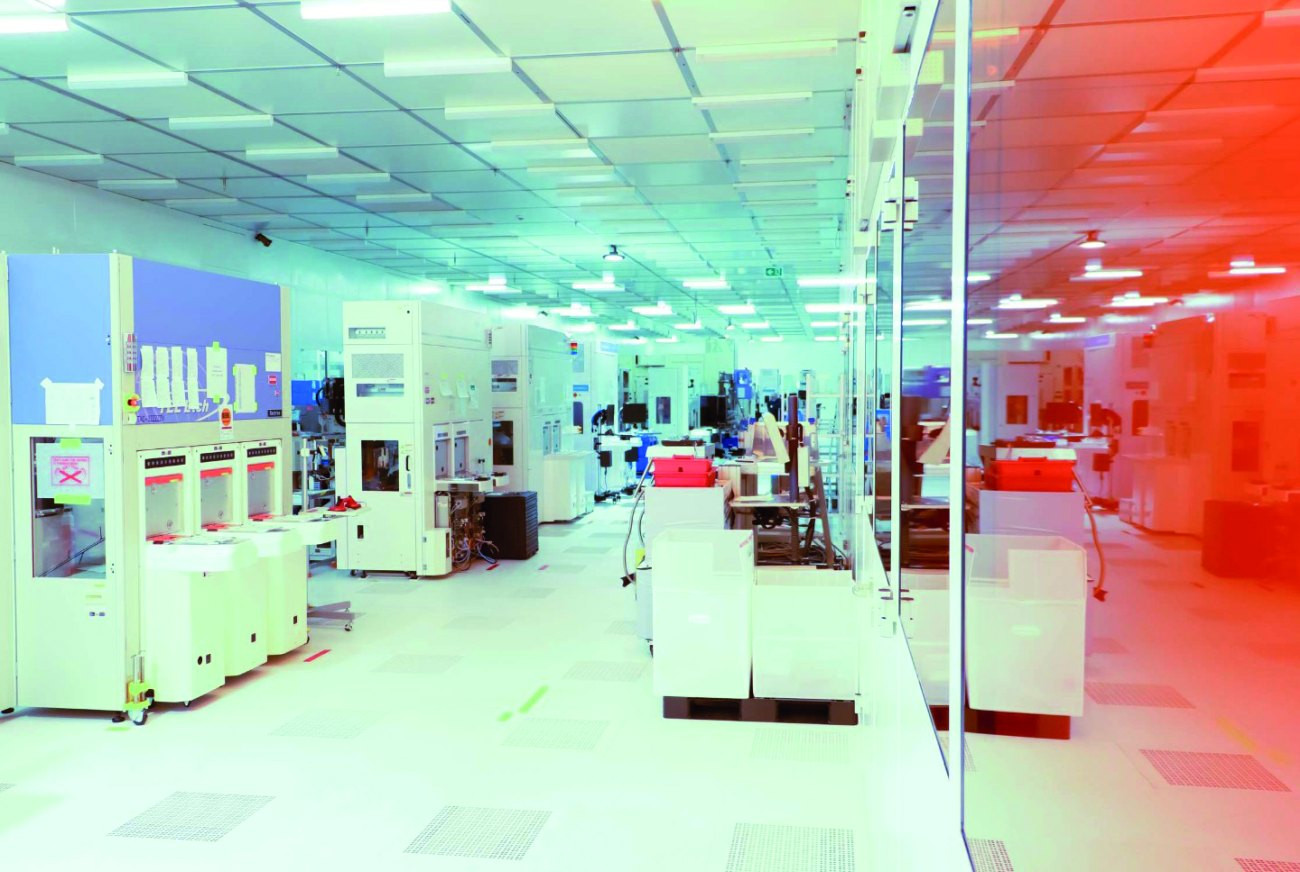 The CNT is working on new nanoelectronic front-end technologies (Image: Paul-Ressl for the FhG-IPMS)
The associated forlabs are working on two-dimensional materials, memristors, spintronics, brain-like computers, new sensors, photonics, better power electronics and high-frequency electronics, among other things. The 'Dresden Microelectronics Research Laboratory for Reconfigurable Electronics' (DCST), for example, is experimenting with chips that can reprogram themselves for new tasks at the hardware level. The funding helped the Dresden-based company to set up a small, complete chip production chain through to final assembly, with which they are working on titanium nanowire transistors, among other things. The purchases included a particularly efficient atomic layer deposition (ALD) system.
Another example from Saxony: the 'ForLab Mat4μ' at the Bergakademie Freiberg is looking for new materials and test components for power electronics, as well as nanodiamonds for quantum computers.
Gap between research and commercialization
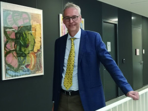 Prof. Karl LeoDespiteall these newly created structures and networks, there are still gaps in Saxony and throughout Germany between the actually strong scientific and technical research landscape and the broad commercial marketing of the knowledge gained there. The USA, and Silicon Valley in particular, has been seen as a role model for years, where top Californian universities and high-tech forges cross-fertilize each other - and generate new disruptive products at certain intervals.
"Germany needs more pilot lines," demands Harald Gossner, for example. He is one of the German chief engineers at semiconductor company Intel, which is currently preparing to build two large chip factories in Magdeburg. He explains: "What we need here is an intermediate step in which we can test whether a new approach is marketable and integrable."
However, as start-up equipment is particularly expensive in microelectronics, this would require considerable investment, which hardly any one location could afford on its own. "These have to be nationwide solutions."
Meanwhile, the Fraunhofer Institutes involved in Dresden are endeavoring to combine their already installed semiconductor development technology into complex, practical pilot lines. The emphasis here is on practical, as these are systems similar to those found in top semiconductor fabs, which can process wafers with a diameter of 300 mm, for example. Specifically, the Free State of Bavaria and the Fraunhofer-Gesellschaft want to bring together the front-end and back-end research, which were previously separated, in one location. The plan is to set up a new 'Center for Advanced CMOS & Heterointegration Technologies Saxony' in the former Plastic Logic electronics paper factory in the north of Dresden. The Fraunhofer Institutes IPMS and IZM are involved in this via their subsidiary centers: the 'Center Nanoelectronic Technologies' (CNT) specializes in front-end processes, while the 'All Silicon System Integration Dresden' (Assid) focuses on the back-end and 3D integration. In this respect, both centers will continue to pursue their existing development paths in a 4000 square meter clean room. In addition, they will focus more than before on chiplets and other heterogeneous combinations of different circuits, sensors and other components in one chip.
Focus on additive circuit packaging
Independently of this new microelectronics research complex, the Fraunhofer-Gesellschaft in Saxony is also pursuing back-end process developments at other locations. One example of this is the Fraunhofer Institute for Electronic Nano Systems (ENAS). It recently set up a new cleanroom laboratory for additive circuit assembly at its Chemnitz site. The engineers there combine various 3D printing technologies that can be used to additively manufacture the electronics themselves as well as conductor paths, housings and other assembly and connection technology. Their aim is to enable German high-tech developers to assemble their electronics prototypes themselves in future without having to go to the large back-end factories in Asia.
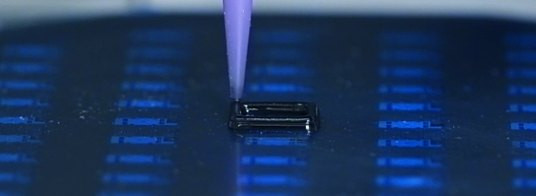 A dam and fill dispenser creates a shell for an electronic component in the Enas clean room. In addition to such dispensing systems, Fraunhofer has combined a variety of modern additive processes in Chemnitz
"Current developments, such as miniaturization, 3D integration and the integration of various functional components in a so-called 'system in package', require new materials and therefore new technologies," said researcher Frank Roscher, explaining why the institute has set up such a cleanroom laboratory.
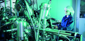 In the ForLab DSCT at TU Dresden, facilities are being set up for interdisciplinary research into circuits made of nanowires (Image: TU Dresden/IHM)The new ENAS cleanroom laboratory combines several such approaches. These include, for example, nanoparticle ink printers, solder paste distributors, special injection molding machines, a cluster system for 3D-compliant material deposition, screen printing and dispensing systems, assembly robots, robots with print heads and other devices. These devices and processes enable the use of nanoparticle inks, chemicals, sensory materials such as CNT pastes as well as solder pastes, electrically conductive and insulating materials, also in combination with each other. As an example of what this makes possible, the Fraunhofer engineers used injection molding to create a gear cap into which they integrated an electrical circuit with magnetic field sensors in order to save space for other electronics.
Speaking of 3D printing: while others are concentrating on additive manufacturing with particularly high-quality materials such as titanium and ceramics, Prof. Henning Zeidler and his team at the Bergakademie Freiberg want to process biogenic waste in industrial 3D printers. In other words, they want to feed the additive systems with straw, shells, husks, paper, peach pits or hazelnut shells and print stage sets or other materials from them. Saxony's Regional Minister Thomas Schmidt is funding a new 'Sustainable Additive Manufacturing in Saxony' (Samsax) laboratory in Freiberg specifically for such approaches, which aim to find new ways of recycling using 3D printing.
Siltronic and FMC: millions invested in wafer production
Speaking of Freiberg: in addition to 3D printing and resource technologies from mining to recycling, the production of wafers made from silicon and compound semiconductors has been a very important pillar of this research and business location since GDR times. The flagship companies in this sector include Siltronic, which supplies industry giants such as Samsung, Intel and Bosch with its silicon wafers, as well as Freiberg Compound Materials (FCM), which specializes in gallium arsenide and gallium nitride as a wafer material, among other things. Both companies have now announced new investments in Freiberg: Siltronic wants to invest a "three-digit million amount" in a new crystal pulling hall and further expansion steps. FCM, on the other hand, plans to invest around €60 million at the site by the end of 2023. Among other things, the company wants to produce its first indium phosphide wafers at the beginning of 2023. The electronics that will later be manufactured on these wafers are primarily intended for photonics and specifically for fiber optic systems.
Photonic innovations have also been made possible by the latest spin-off from the Institute of Applied Physics at TU Dresden: in the start-up 'Phosphorescent Response Under UV Excitation' (Pruuve), three physicists want to produce and sell innovative rewritable luminescent films. Using individually designed organic layers in a plastic coating, they can display UV doses particularly accurately in industrial processes. "For the first time, our UV sensor films enable precise measurement of the UV dose directly on the surface and during the manufacturing process," emphasizes Dr. Paul-Anton Will, co-founder and product developer at Pruuve. "We thus offer a reliable and fast success control for UV curing and UV disinfection. Companies can thus avoid unnecessary waiting times, reduce their energy costs and also reduce material wear."
The founders still see great prospects for their films. They can not only be used as a kind of UV dosimeter, but can also be rewritten and erased again and again with mask support and infrared light. In this respect, they can also be used in future to produce reusable labels and security seals that are only selectively visible to selected companies in a product's long value chain.
Charging smartphones with body heat
The Institute of Applied Physics, which has already produced Novaled, Heliatek and numerous other organic electronics spin-offs in the past, is currently researching a new project that could potentially produce a particularly ambitious spin-off: Dresden's organic electronics pope Prof. Karl Leo and his partner Dr. Shu-Jen Wang are currently working on organic energy harvesters (energy harvesting), which in future will recharge smartphones, smartwatches and other mobile devices using body heat alone. The scientists are modifying thin-film crystals made from the red organic dye rubrene using modulation doping. "Our results show that modulation doping in combination with highly mobile crystalline organic semiconductor films represents a novel strategy for achieving high-performance organic thermoelectrics," emphasized Dr. Wang. Prof. Leo sees great potential in this approach because the thermoelectric converters created in this way are flexible and yet comparatively efficient at generating electricity from body heat: "Our work paves new paths to flexible thermoelectric devices that make it possible to generate electrical energy directly from heat in an elegant and efficient way."
Artificial hair: robots anticipate approaching touches
A new robot skin from Chemnitz University of Technology is hardly less ambitious: it senses approaching touches using artificial hairs that are modeled on human body hair. This facilitates collaborative work between robots and humans in industry, for example. These small sensor hairs in the robot skin can even detect the direction from which a human touch is approaching. This brings the electronic skin a big step closer to the real touch sensitivity of organic skin, according to a press release from Chemnitz University of Technology, which has driven this project forward together with the Leibniz Institute for Solid State Research (IFW) Dresden. The scientists produced these small sensors using the so-called micro-origami technique. This involves first creating the sensory and electronic components in two dimensions and then folding up the flexible carrier material in the same way as Japanese paper technology. With this method, many microelectronic components fit into a very small space with geometries that cannot be realized with conventional microchip manufacturing processes.
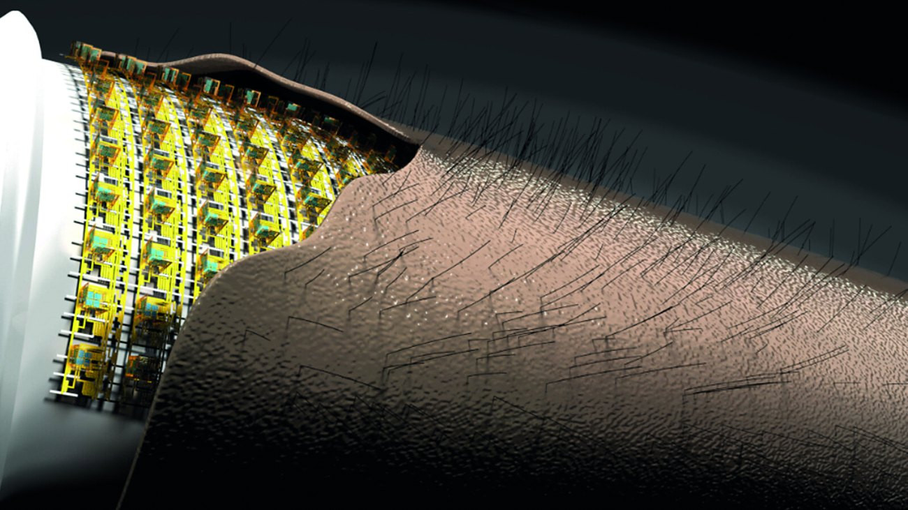 Artificial electronic skin (e-skin): Highly integrated flexible microelectronic 3D sensor technology detects the movement of hairs on artificial skin (Graphic: Research group Prof. Dr. Oliver G. Schmidt)
The electronic skin itself consists of a flexible polymer plastic into which the researchers integrate proximity sensors and other electronic components - similar to the nerves and sensory cells of natural skin. Their latest coup is the artificial hairs with magnetic field sensors at their roots. These tiny anisotropic magnetoresistive sensors (AMR) can detect changes in the magnetic field particularly precisely and three-dimensionally. The idea is that if the artificial hairs on the robot skin bend in one direction or another, for example because a human hand is about to pass a screw or component to the robot, the sensor registers these small changes in direction even before the human hand touches the robot hand in the next millisecond. The robot can then slow down or stop its own movements in good time or activate spring functions so that the human colleague does not sustain any bruises from the steel hand.
Sources:
Silicon Saxony, oiger.de, TUC, TUD, Fraunhofer Enas, Fraunhofer IPMS, Fraunhofer IIS, IAPP, Bergakademie Freiberg, FMD, Pruuve


