![Better safe than sorry[1]](/images/k2/ab30cb672d4889e3e3a0c702e06338e2.jpg)
It's a truism - in journalistic jargon 'a truism' for short: mistakes cost you dearly. So it is fair to ask why no effort is made to avoid errors - especially since in many cases we know what causes errors in an electronic production.
In production, perhaps one of the main reasons for the ignorant attitude towards errors is an organizational approach advocated by many 'business schools': Establishing cost centers. This largely puts a stop to cooperation between individual departments. With 'competition is good for business' and the associated incentive to reward particularly cost-effective solutions, the result is that walls are built instead of cooperation being sought.
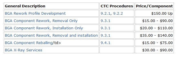 Fig. 2: Price list of the Circuit Technology Center, Haverhill, MA, USA
Another reason may be that many manufacturers do not calculate individual products separately and therefore the costs that accumulate during repairs are spread over the total quantity. As a result, management does not realize, if it pays attention at all, that individual products that run through a repair loop - in some cases they are even trapped in it - are much more expensive than those that are produced without defects.
The often pampered development engineers look down on the process engineers, because they don't sit in air-conditioned offices, but have to move around in the 'dirty' (as they are probably seen, as they have never ventured into these areas) environment of machines and materials. They are reluctant to smear their fingers with disgusting flux, for example. Instead, they sit in comfortable office chairs in front of their computer screens and work up a thick callus on their buttocks.
 Fig. 3: Visual inspection is no longer sufficient for modern productsFaultsin production are expensive due to the loss of a finished or semi-finished product or the cost of reworking. The days of quickly removing a solder bridge with a hot soldering iron are long gone. With PCBs that are fitted with extremely small components and dozens of large BGAs, you can't get any further with this kind of 'fiddling around'. The necessary troubleshooting alone is time-consuming and requires a high level of expertise, because even the best X-ray systems still suffer from their software: the α and β errors, i.e. the overlooked and incorrectly displayed errors, still make up a high percentage and must be assessed by an 'expert', because artfully removing and successfully replacing a large BGA requires sensitivity, a good device and, of course, a lot of time - something you don't want to do unnecessarily.
Many incidents can be avoided as early as the PCB design stage. The rejection of the PCB is not only due to the chosen material but also to the thermal distribution. Good designers know how to balance metallization and, if necessary, this requires additional and non-functional copper areas. Attention must also be paid to the distribution in the layers.
There are plenty of guidelines on the Internet on how to lay out solder pads so that midchip solder balls, for example, hardly ever occur. This also applies to the various BGAs and SOTs, so that specific soldering errors can be largely avoided.
Among the numerous end surfaces, it is also possible to select those that can be best processed in production, which takes into account parameters such as shelf life and coplanarity.
As the purchasing department has often never heard of solderability, let alone knows how to test it, they are happy to buy the cheapest scrap on the component market, as this increases the buyer's Christmas bonus. Specifications on dimensions, cleanliness, solderability, metallization, etc. etc. could probably provide some relief here and reduce the overall costs despite more expensive components. A few months on the line for the men and women certainly wouldn't hurt either.
Successful measures also include spot checks carried out by qualified inspectors on receipt of the goods. Similar measures also apply to other goods such as pastes or fluxes.
Unless prescribed by 'higher' authority, a studied choice of paste can eliminate many potential problems. In addition to 'blowholes', which can be greatly reduced, wetting, contamination and the durability of the solder joint can also be adjusted. A good laboratory or cooperation with an external one as well as relevant tests - especially with the products to be manufactured and short series in the current system - help to find the 'best' paste.
 Fig. 4: X-ray image - far too many errors!Staged stencils can often be avoided or greatly simplified at the PCB design stage if the design engineer knows her trade, because even normal stencils are critical. When specifying them, attention should not only be paid to the metal or the manufacturing method (laser-cut and skillfully polished often perform best in relevant comparisons), but also to the shape of the openings (e.g. rounded corners), the size and arrangement of which, if chosen correctly, help to reduce errors. However, it is not yet clear whether the new coatings are really helpful, as many are so thin that they are no longer detectable after a short time.
Numerous parameters have to be taken into account when printing. Although paste printing is now proving to be a bottleneck in large-scale production, the feed rate of the doctor blade should not be too fast. Closed doctor blade systems are particularly undesirable for difficult print patterns, as they have to be filled with particularly thin pastes, further reducing the already rare amount of metal that remains on the pad.
Today's lead-free alloys and pastes are more critical, as the high melting temperatures do not allow ideally suited (largely non-toxic) chemicals for the fluxes and, on the other hand, can attack thermally labile components. For this reason, the specifications for heat application in reflow ovens have changed considerably for the assemblies. There are changes in heating and the dwell time above the melting point, and the paste manufacturers' suggestions are often anything but realistic or even feasible. Only test series and a better knowledge of the process engineer or additional research in the trade press or at conferences can help here.
This approach, which requires the willingness of the various groups to work together, can significantly increase the initial yield and substantially reduce the overall costs of manufacturing electronic devices, which in the end hardly benefits the workers but at least the shareholders.
A completely error-free production as propagated by some gurus is of course illusory and so the aim is to achieve an error level at which it is cheaper to dispose of the faulty product (in an environmentally friendly way) instead of repairing it at great expense, which is also good for quality.
Literature and notes
K. Bryant; M. Popovics: An Interesting Approach to Yield Improvement, SMTA Proceedings
C. Tudor: Minimizing Voiding, Indium Corporation; 2017
C. Tafoya et al: Assessing the Effectiveness of I/O Stencil Aperture Modifications on BTC Void Reduction, PC APEX EXPO Proceedings
H. Grumm; D. Graupner: The Potential of Stencil Technology - Choosing the Right Stencil Options to Maximize Yield and Earnings, SMTA Proceedings
K. Sweatman et al: Controlling Voiding Mechanisms in the Reflow Soldering Process, IPC APEX EXPO Proceedings
L. Bruno; T. Johnson: Printing of Solder Paste - A Quality Assurance Methodology, IPC APEX EXPO Conference Proceedings
B. J. Leach: Defect free QFN Assembly, AccuSpec Electronics, LLC, 2011
References:
[1] Johann Christoph Ettner von Eiteritz: Deß Getreuen Eckharts unwürdiger DOCTOR, Augspurg und Leipzig, bey Lorentz Kroniger und Gottlieb Göbels Seel. Erben, bookseller, 1697, p. 286
