
Although you cannot tell the taste of the contents from the size of the cup, the connoisseur knows that an Italian espresso or Turkish coffee, for example, is served in smaller cups or glasses than a latte or a Pharisee [1]. I will bypass other discussions about the title here and focus on electronic production.
Many things are getting smaller and smaller there - often simply for 'fashion reasons' or because the applications require it: For example, in so-called 'smart' handheld phones, which are now being upgraded to 5G, which entails larger antennas and also thicker batteries whereby the device should not become larger.
 Fig. 2: GRM011R60J104M from Murata - a multilayer ceramic capacitor with a maximum capacitance of 0.1 μF. Nominal voltage of 6.3 VDC; temperature range from -55 °C to 85 °C; size 0.25 x 0.125 x 0.125 mmThebest 'smartphones' contain up to 1000 components that somehow have to be accommodated in a limited space. It helps if the components are also smaller. Component manufacturers see this as an opportunity to make money again and so Murata has announced the sale of ceramic capacitors [2] that are as small as a grain of sand. Buyers will be pleased, as they can now incorporate additional functions such as the dreaded face scanning to unlock the screen, which is praised in Japan but demonized in China, or ignoring calls from a beloved friend by simply gesturing defensively with her hand in front of the device.
This has far-reaching consequences, for example in production, where you have to think about how to get these grains of sand onto the circuit board and how to solder them.
Such small components place high demands on the placement machines. Therefore, an exceptionally stable frame with a high-precision drive is essential for the machines. The image processing system should be able to illuminate the components with different qualities of light in order to take into account differences in the component suppliers. Integrated suction air flow detection should be part of the pneumatics in the placement head to monitor the presence of the component from pick-up to placement. Certain other functions are desirable, such as adaptive pick control and automatic recognition of individual feed types. If the thickness of the chips is also recognized and measured using a CCD camera, the placement can be controlled more precisely and thus the yield during placement can be improved.
0.125 mm corresponds to 125 µm. If you look at the grain size of the metal particles in solder pastes - according to the classification of the contemplative IPC - then in the worst case two class 3 grains already make up the thickness of the component. This results in a truly untenable condition during printing(Table 1).
The consequence is therefore to switch to pastes with a smaller grain size(Tab. 2). Paste type '5' or even '6' are now available, but have certain disadvantages, such as an increased proportion of metal oxides, as the total surface area available to oxygen is greatly increased by the smaller spheres. When moving from IPC class '3' to class '5', the metal surface area roughly doubles, and more than triples for class '6'(Table 3).
Tab. 1: Specification of solder grain sizes according to IPC J-STD-005A
|
IPC Type |
Less than 0.5 %, more than (mm) |
10 % max. between (mm) |
80 % min. between (mm) |
10 % max. less than (mm) |
|
3 |
60 |
45 - 60 |
25 - 45 |
25 |
|
4 |
50 |
38 - 50 |
20 - 38 |
20 |
|
5 |
40 |
25 - 40 |
15 - 25 |
15 |
|
6 |
25 |
15 - 25 |
5 - 15 |
5 |
Tab. 2: 5-grain rule for openings in a stencil
|
Paste type (according to IPC) |
Size range of the grain size in µm (80 %) |
Minimum size of the opening in mm |
|
3 |
25 - 45 |
0,2286 |
|
4 |
20 - 38 |
0,1905 |
|
5 |
15 - 25 |
0,1270 |
|
6 |
5 - 15 |
0,0762 |
Tab. 3: Rule of thumb - 5 grains fill the width of the opening
|
IPC type |
Average area of 1 kg (m2) |
Normalized area |
|
T3 |
22,9 |
1,00 |
|
T4 |
27,7 |
1,21 |
|
T5 |
40,2 |
1,75 |
|
T6 |
80,3 |
3,50 |
Although inert gases are used in the production of the powders, oxidation cannot be completely ruled out during further processing. The paste manufacturer tries to counteract this with various acids and chemicals, which is helpful on the one hand. On the other hand, the residues are increased after soldering, which means that subsequent cleaning is almost always necessary for critical products.
It should not be overlooked that oxidation also takes place during soldering, and faster than at lower temperatures. The 'head-in-pillow' defect or increased solder beads as well as 'graping' - i.e. the appearance of grapes - provides striking proof of this.
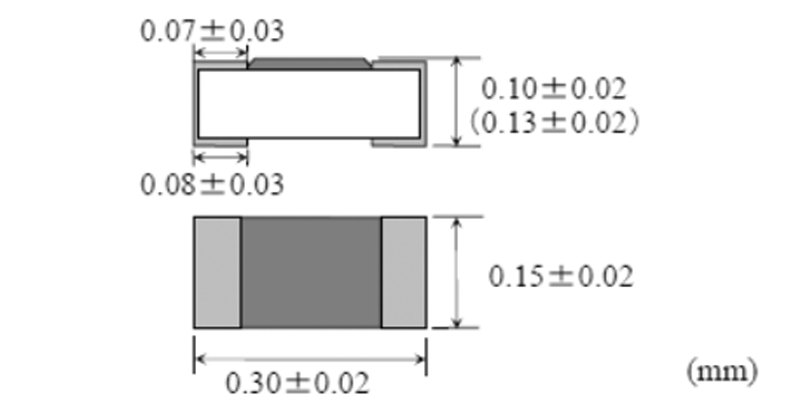 Fig. 3: Target size of a 03015M component
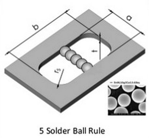 Fig. 4: Size of the metal surface for different grain sizes
How uncertain the manufacturers are about this can be seen from information such as the oxide content of 'good' pastes. Here, values of 50 to 200 ppm are quoted, whereby it is striking that even four times this amount of metal oxide is said to be acceptable. The question should then be allowed: Why make an effort when even more can be sold at increasingly expensive prices? After all, the prices for finer pastes spiral upwards quite quickly [3].
Nowadays, the shot tower process [4], which was once used to produce shot pellets for the military and hunting, is rarely used in the production of powder. Instead, methods are used that break up the molten alloy using a gas jet, a rapidly rotating disk or ultrasound. The quality achieved varies and in order to obtain as few particles as possible that deviate from the spherical shape, the production process must be carefully controlled, as subsequent sieving and sorting steps are not able to specifically remove such out-of-round grains.
Although a better print result can be achieved with finer-grained pastes, this comes at the cost of other disadvantages, including reduced shelf life.
As anyone with a printer will quickly realize, you cannot achieve an acceptable print with a 'proper' paste alone. Too many factors come into play here. In addition to the printer itself, of course, the stencil and the many parameters that have to be chosen favorably. The PCB with its layout, the arrangement of the components on it and the solder resist are further details that need to be taken into account.
The smaller the components and the smaller the gaps, the more difficult it will be to apply enough paste for a durable solder joint. If the assembler then crushes the paste, all efforts will have been in vain.
If the dear process engineer now thinks that another method of solder application will be more successful, such as 'jetting' - the solder spraying process that is just becoming modern - she may be disappointed, because at least one study indicates that cleaning afterwards is even more difficult than after stencil printing.
Literature:
B. Fischthal, M. Cieslinski: Beyond 0402M Placement: Process Considerations for 03015M Microchip Mounting, IPC APEX EXPO Conference Proceedings
T. Lentz: Size Matters - The Effects of Solder Powder Size on Solder Paste Performance, SMTA Proceedings
IPC-7351, Generic Requirements for Surface Mount Design and Land Pattern Standard
T. O'Neill, K. Seelig: Solder Paste Powder: When to Downsize - A finer type solder paste may solve one problem only to create another, Circuits Assembly
M. Bixenman et al: Stencil Printing Yield Improvements, SMTA Proceedings
R. Parthasarathy et al: Jet Printed Solder Paste and Cleaning Challenges, Proceedings of IPC APEX, February 2018
References
[1] https://de.wikipedia.org/wiki/Pharis%C3%A4er_(Getr%C3%A4nk)
[2] https://www.electronicdesign.com/analog/one-smallest-components-smartphones-shrinks
[3] https://www.somersetsolders.com/soldering/solders-and-fluxes/solder-pastes/c35: Qualitek 825 Lead Free Solder Paste T3 = £33.46; Almit Lead Free Solder Paste T4 = £87.95
[4] Invented by William Watts and patented in 1782
