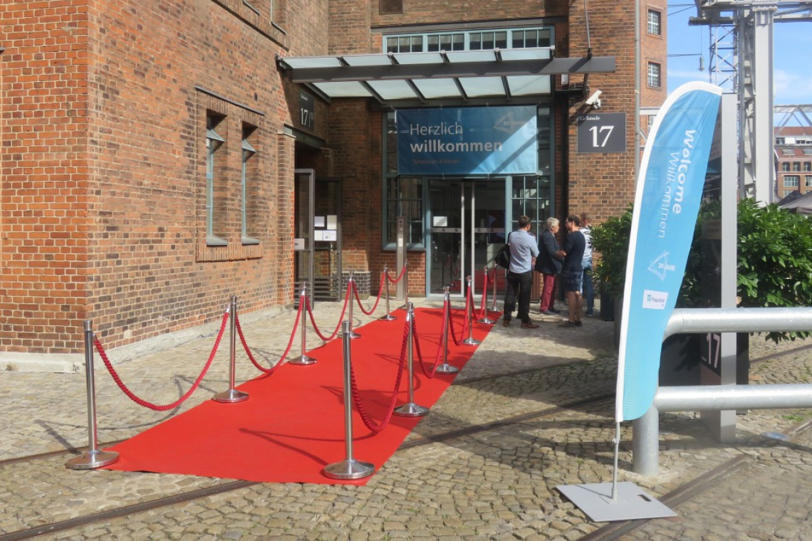
The Fraunhofer Institute for Reliability and Microintegration IZM celebrated its 30th anniversary in September. It organized the international symposium 'Crossing Frontiers in Microelectronics' followed by a ceremony and get-together.
 The Fraunhofer Institute for Reliability and Microintegration IZM is based in a historic building in BerlinTheresearch institute, which today employs over 400 people at three locations, wasfoundedby a group of 21 scientists from Germany. In 1987, Professor Herbert Reichl took over the Chair of Microperipheric Technologies at the Technical University of Berlin. Microelectronic technologies were also developing rapidly in Germany at the time, but the gap between ever smaller circuits and inefficient packaging was wide. The focus therefore had to be placed more on assembly and connection technology and chip manufacturers and applications from industry had to be brought together. The idea to establish the Fraunhofer Institute for Reliability and Microintegration IZM was born.
The history - building, connecting and integrating
Under the leadership of Herbert Reichl, a group of scientists from the TU and HU Berlin and the Academy of Sciences in Chemnitz came together and succeeded in reuniting research from West and East Germany in December 1993. The Fraunhofer Research Institution for Reliability and Microintegration was launched with the mission of developing competitive packaging and interconnection technology for industry. This was to be achieved through technologies that did not yet exist in Europe and would open up completely new fields of industrial application for chip manufacturers. The aim was to establish Germany as a center of science in microelectronics. The first cooperation agreement was concluded with the research focus 'Microperipheric Technologies' at TU Berlin, and the institute also worked closely with the university in terms of personnel.
The first coup was already achieved in the founding year
For the first time in Europe, the use of low-cost polymer printed circuit boards for flipchip assembly was investigated for more cost-effective production. In flipchip assembly, unhoused semiconductor chips are turned over and connected to a substrate with the entire active contacting side by means of so-called bumps instead of wire connections. This process significantly reduces the cost of bumping individual wafers and the space required on the chip. Just two years later, the scientists put the first flipchip assembly line into operation in Europe and worked together with leading equipment and device manufacturers to demonstrate the possibilities of this technology. Due to its great success in industry and science, IZM was granted official institute status and thus fully established within the Fraunhofer-Gesellschaft.
 Prominent participants followed the ceremony
First prominent application of flipchip technology
The first prominent application of flipchip technology came in 1997 with research into the use of pixel detectors in particle accelerators and has been the basis of the collaboration between CERN and IZM to this day. At that time, the employees produced a demonstrator for a detector module based on flipchip technology, which was then used at CERN. The flipchip line demonstrated that IZM's technology could be integrated into a production line for surface-mounted technology (SMT) and was therefore ready for introduction in industry. Thanks to such a prime example, many SMEs became customers of the institute.
Various locations, personnel and turnover built up
 AVT experts discuss during the coffee breakAtthe various locations, not only the staff but also new subject areas were built up: in 1998, for example, a department and branch office was established in Teltow and expanded the institute's portfolio to include polymer materials and composites. In the same year, a project group was founded in Paderborn in collaboration with the university there and cooperation with Chemnitz University of Technology was strengthened, so that a department was established there in the field of microsystems technology and microsensor technology, which has been independent since 2008. Similarly, from 2002 onwards, IZM developed its Munich branch to such an extent with roll-to-roll and 3D wafer technologies that it has since become an independent institute.
After just ten years, IZM has grown from just under 20 to over 200 employees and its turnover from DM 1.4 million in its founding year to € 27.3 million in 2004.
Integration of applications in electronics
From 2003, the focus increasingly shifted to the integration of applications into electronics. New materials that are more stretchable and flexible are still being tested today. The market for wearables and smart textiles was born and remains an important pillar of the institute to this day. At IFA 2005, employees presented clothing with integrated communication systems for the first time. This included a solution for bicycle couriers that integrated order processing, tracking and navigation.
The institute continued to develop in line with the applications and integrated itself into sectors such as automotive and industrial electronics, medical technology, ICT and semiconductors. In 2010, the All Silicon System Integration Dresden (ASSID) center, which still exists today, was founded in Dresden. The department, in which employees in Berlin and Dresden work together, has clean rooms and laboratories with state-of-the-art production-compatible equipment at both locations. In addition to particular flexibility in the processing of different wafer sizes, both process lines are characterized by the fact that they can be individually adapted to specific process conditions. In 2010, this enabled the development of a microcamera that is no larger than coarsely ground salt and therefore fits perfectly into an endoscope tip. This breakthrough in medical technology was due to a sophisticated assembly technique in which the optics and sensor are integrated at wafer level.
Start-A-Factory - a unique prototype line
After 20 years of existence, further continuous growth and now under the leadership of Prof. Klaus-Dieter Lang, IZM founded the Start-A-Factory in 2017, Berlin's unique prototype line consisting of device infrastructure and a working environment specifically designed to meet the needs of hardware start-ups and the development of their prototypes.
Reliability and sustainability right from the start
IZM is also addressing the issue of sustainability and resource scarcity in the ongoing large-scale project called 'Green ICT' in order to optimize the sustainability of information and communication technology (ICT), whereby the expertise of life cycle assessments and sustainability studies has been part of the institute's name from the very beginning. Reliability not only stands for stable cooperation between research and industry, but also for durable electronics that are designed to be sustainable right from the production stage. The sustainability experts at IZM have therefore been working with leading ICT companies for years and have also contributed to the development of the Fairphone - the smartphone that focuses on longevity and not buying a new one after the next update.
Today, over 400 employees under the leadership of Prof. Martin Schneider-Ramelow are tackling new challenges such as the chip shortage, increasing data rates, the energy crisis and much more. They are developing processes and technologies for quantum electronics, 6G, zero-power electronics and high-performance systems in unusual applications and for harsh environmental conditions.
The scientists and the administrative team have retained one thing: The spirit of wanting to discover new things and push physical boundaries in the process. The symposium to mark the 30th anniversary is to be understood entirely in this spirit: "Crossing Frontiers in Microelectronics", researchers showed which boundaries they want to make disappear in the coming decades.
Symposium shows where developments are heading
Dr. Tanja Braun, Fraunhofer IZM, acted as moderator and welcomed the participants. She gave a brief review of the origins of the historic building in which the IZM is based in Berlin.
Dr. Isabelle Ferain, GlobalFoundries, then explained the Semiconductor Foundries View on Heterogenous Integration. Partnerships with an R&D ecosystem and personnel development are important for further development. Using the example of Si photonic chips and GaN for power electronics, she illustrated what is required for 3D heterogeneous integration in terms of materials, components, processes and functions. These include interposers, TSV and die-to-wafer bonding.
Dr. Michael Schiffer, Fraunhofer IZM, looked at advanced packaging for high-performance computing applications, starting with the challenges. The development goes from the CPU to the GPU to the TPU. SoC or, more cost-effectively, chiplet structures can be considered for implementation. New technologies for TSV, interposers and ultra-fine pitch bonding are being investigated, including microbumps based on nanoporous gold.
 Dr. Tanja Braun during the welcome speech
 Dr. Isabelle Ferain looked at hetero-integration
 Dr. Michael Schiffer looked at advanced packaging for high-performance computing
Dr. Stefan Ruebenacke, Bosch Sensortec, informed about sensor systems for leading edge consumer applications. With a daily production of 4 million MEMS at its plant in Reutlingen, Bosch is the market leader in smart sensors. These have advantageous properties for many applications, as illustrated by typical examples ranging from hearing aids to drones.
Dr. Michael Kaiser and Dr. Julia-Marie Köszegi, Fraunhofer IZM, presented integration solutions for modular communication electronics of the fifth and sixth generation based on general module design options at IZM. Integrated antennas, which are realized as antenna-in-package (AiP) modules based on PCB embedding or mold embedding, are a solution for millimeter waves and sub-THz frequencies. For these frequencies, the signal path design and material characterization is a particular challenge. The EU project SERENA has developed a platform for next-generation systems that offers significant improvements in terms of energy efficiency, costs and functionality.
|
|
|
|
| Dr. Stefan Ruebenacke, Bosch Sensortec GmbH, provided information on sensor systems |
Dr. Michael Kaiser and Dr. Julia-Marie Köszegi presented integration solutions for communication electronics |
|


 Karsten Schischke showed possibilities for reducing theCO2 footprint of electronicsProf. Friedel Gerfers, Technische Universität Berlin, spokeabouthighly integrated, energy-efficient microelectronic systems for future optical and mobile applications. He focused on how the necessary energy efficiency improvements can be achieved and listed relevant projects. The trend is moving from QSFP modules to co-packaged optics (COBO) for thermal management reasons.
Prof. Eckart Hoene, Fraunhofer IZM, discussed the technology trends in power electronics. New solutions are being sought for ever faster switching electronics. Reducing material consumption for each power electronics unit is the key to resource efficiency and cost competitiveness. PCB and molding-based packaging are promising for mass production.
Robert Giertz, AEMtec, demonstrated the path from feasibility to a marketable advanced package. He presented his company, which works closely with the IZM, and its range of services and equipment. The company's own UBM system will be put into operation next. Fan-out wafer-level packaging will also be transferred and should be in-house by 2025, with the exception of RDL.
In response to the question: 'Will microintegration put us on the 1.5° path?', Karsten Schischke, Fraunhofer IZM, used examples to illustrate the current situation and possible improvements. For example, 40% of theCO2 footprint of labtops comes from the semiconductors used in them. This is a challenge for HL manufacturers. Karsten Schischke also addressed the issue of the circular economy with the increasingly high level of product integration, which is favorable for theCO2 footprint. This is because there are interactions between reparability, service life and energy consumption (energy label). Improvements can be achieved with SoC packaging and embedding. Microintegration and electronics as well as digitalization can enable the reduction of greenhouse gases in applications, but depending on the use case, a technological solution can be disadvantageous or advantageous. It is recommended to use the potential of packaging to achieve better performance with less semiconductor usage.
 Prof. Eckart Hoene discussed the technology trends in power electronics
 Prof. Friedel Gerfers provided information on microelectronic systems for future optical and mobile applications
 Robert Giertz showed the way to the Advanced Package
Ceremony with acknowledgements, a tribute, a list of highlights and an outlook
After the welcoming address, Prof. Martin Schneider-Ramelow, Fraunhofer IZM, reviewed the history of the institute as well as its projects and key developments. He ended his speech with praise and thanks for the many years of successful collaboration with customers, sponsors and partners from other institutes.
This was followed by words of welcome from:
- Prof. Axel Müller-Groeling, Director of Research Infrastructures and Digitization at the Fraunhofer-Gesellschaft
- Dr. Henry Marx, State Secretary for Science and Research, Berlin
- Dr. Roland Krüppel, Department of Electronics and Autonomous Driving; Supercomputing at the Federal Ministry of Education and Research
- Prof. Geraldine Rauch, President of the Technical University of Berlin
- Dr. Axel Kaschner, Senior Vice President Corporate Research, Advanced Technologies Robert Bosch
To conclude, Prof. Martin Schneider-Ramelow's success story of the IZM included Ni-Under Bump metallization, embedding, the micro camera and smart sensor systems, and then went into the institute's future mission: With the Chips Act, a platform for hetero and chiplet integration is also required. IZM's vision here is high-end performance packaging.
Since the pandemic prevented a celebration at the handover of the institute's leadership from Prof. Klaus-Dieter Lang to Prof. Martin Schneider-Ramelow, the award was presented retrospectively.
Before the get-together, the Fraunhofer IZM Center All Silicon System Integration Dresden (ASSID) also presented the host with a specially designed wafer to mark the anniversary as a thank you for the collaboration.
 Prof. Martin Schneider-Ramelow with his success story
 Prof. Klaus-Dieter Lang thanked everyone
 ASSID thanked him with a wafer
The pictures
All pictures: Gustl Keller
