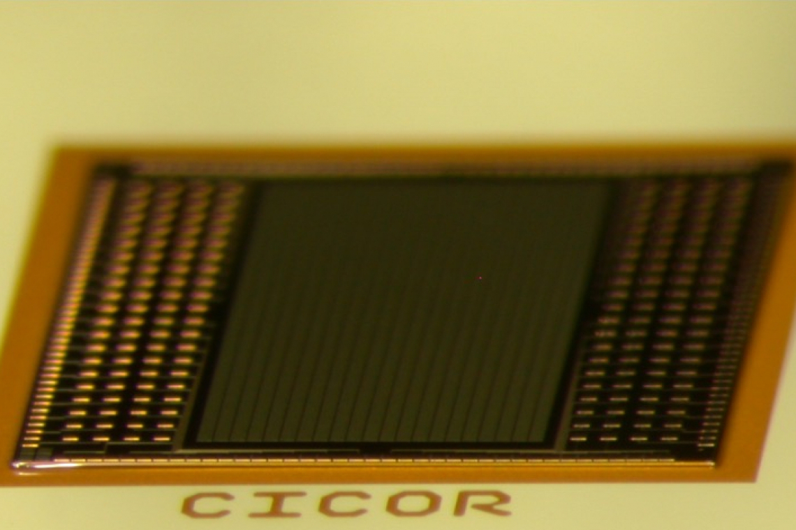
Chip bonding and equipment
At Cicor in Radeberg, chip bonding is an important process for mounting chips on surfaces with different properties. A wide range of die sizes and thicknesses as well as different materials, surface finishes and delivery forms can be processed. Chip bonding can be carried out either manually or fully automatically on a chip bonder.
The fleet of chip bonders at Cicor in Radeberg has been expanded in recent years. Over the years, special requirements have led to the acquisition and use of manual, semi-automatic and automatic chip bonders. The automatic chip bonders are mainly used in ISO5 and ISO7 cleanrooms, depending on the cleanliness requirements of the products to be processed. Among other things, they are used for handling special chips in series production (very thin chips <30 µm thick or small chips up to 0.1-0.15 µm edge length).
In addition to good placement accuracy (Cmk with up to ±7 µm@3s), stable pick & place processes, assembly directly from the wafer or pre-sorted from waffle packs, automatic optical recognition and much more are also important.
In addition to the automatic chip bonders, Cicor also has manual chip bonders for high-precision positioning of optical chips or fiber optic panels (FOPs) for low-volume production. With these manual bonders, better placement accuracies of up to ±3µm@3s can be realized.
Quality checks during chip assembly
Mechanical, optical and radiographic tests (X-ray) are carried out during the process to check the quality of assembled components. These tests and inspections are based on general standards such as MIL-STD883, ESCC/ECSS space specifications or on various customer specifications with individual requirements. Important quality criteria for chip bond connections are, for example, mechanical shear strength, optical criteria such as adhesive or solder wetting, surface contamination, the positioning accuracy of chips and, in the case of soldered connections, the proportion of defects in soldered connections.
Connection technologies in chip assembly
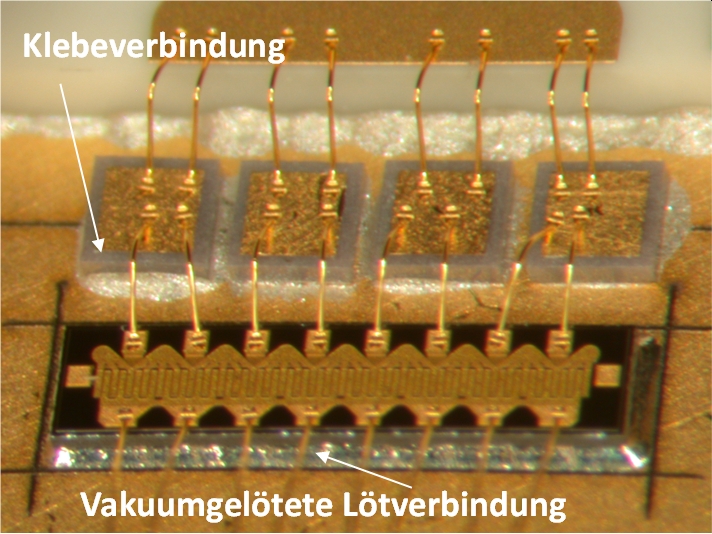 Fig. 1 Chip bonding: Soldering and bondingCicoroffers three technologies for mounting chips on wiring carriers such as ceramic substrates, on PCBs or in housings. Depending on the type of connection technology, they are divided into bonding, soldering and sintering. Bonding materials such as adhesives, solders and sintering pastes are used.
a) Adhesive bonds
Different types of adhesive are used for bonded joints depending on the product and customer requirements. These can be roughly divided into electrically conductive or non-conductive, thermally conductive, filled or unfilled, 1K or 2K, and according to the type of curing mechanism. As the adhesives are mainly available in the form of pastes, they can be applied using various methods such as dispensing, stamping or screen printing, depending on their viscosity and properties.
In order to achieve good results in the bonding process, the quantity and distribution of the adhesive used must be adjusted appropriately during assembly, taking into account properties such as adhesive viscosity, chip size, chip aspect ratios and the wetting behavior of the surfaces.
For a good bonding result, it is necessary to use application patterns adapted to the respective chip and substrate for the application of adhesives (see Fig. 2). For small chips, only individual dots or a small dot matrix are usually used due to the small amount of adhesive required. For larger chips with varying aspect ratios, other patterns such as lines, bones or snowflakes must be used in order to apply a sufficient amount of adhesive in a reasonable amount of time and to achieve good adhesive distribution among the chips and a good wetting result. The dispensing results also depend significantly on the type and size of the dispensing needle used and on process parameters such as pressure/time, traversing speed or predefined volume.
After the adhesive has been applied and the chips have been loaded, it is necessary to cure the adhesive.
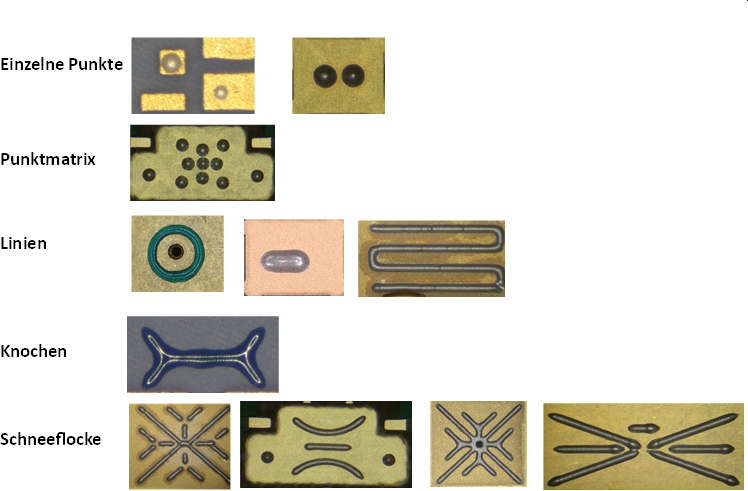 Fig. 2: Different patterns of adhesive application depending on the requirementsDependingon the requirements of the materials/products and their construction, different adhesives with different curing mechanisms such as temperature, UV light, self-crosslinking or moisture are used. Typical curing temperatures for epoxy resin adhesives, for example, range from room temperature up to 150°C.
b) Vacuum soldered joints
Another method of chip assembly is vacuum soldering. This soldering process is known for its good cleanliness, as no flux is used in the solder in contrast to the standard reflow process with solder paste. The cleanliness of the chip surfaces, without the need for additional cleaning steps, is an essential prerequisite for good processability of the assembled chips in subsequent processes such as wire bonding, for example for aerospace products.
The solder material is usually applied in the form of solder preforms (pre-cut metal foil), pre-applied remelted and cleaned solder deposits or as vapor-deposited solder layers. Vacuum brazing mainly uses brazing alloys such as AuSn, SnAgCu, SnIn, SnBi or PbSn brazing alloys for aerospace applications.
Many types of ceramic and metallic materials are suitable for vacuum brazing as they are temperature-resistant and low in outgassing. Depending on the temperature load during soldering, plastics are not used if possible, as they can contaminate the vacuum process due to outgassing effects.
The correct positioning of the chips during soldering is ensured by the use of soldering barriers such as mechanical steps, milled or lasered lines.
Typical solder melting temperatures range from 130°C to 290°C, depending on the solder alloy. Possible brazing temperatures of up to 400°C at low chamber pressures of up to 0.1mBar can be realized in a vacuum brazing furnace.
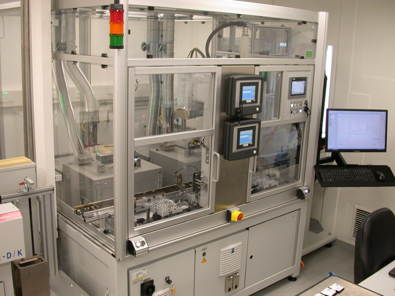 Fig. 3 Fully automatic batch vacuum brazing systemAfully automatic batch vacuum brazing system with two brazing furnaces and robot handling is shown in Fig. 3. The robot picks up the workpiece carrier with the soldering material at the loading position of the transport section and moves it from the loading position directly into the vacuum soldering chamber. The transport of the workpiece carriers must be very precisely coordinated and free from vibrations or impacts in order to avoid uncontrolled movement or misalignment of the components to be soldered, as these are only stacked loosely on top of each other. The vacuum brazing process starts automatically as soon as the chamber is closed. After soldering, the unloading process is carried out in the same way.
The quality of the vacuum-brazed solder joints is checked with each production order using a separate X-ray inspection. The proportion of defects in the solder, the wetting of the solder and the positioning of the chips are important quality criteria that are assessed using the X-ray images. The soldering results are significantly influenced by the process control, the soldering profile, the cleanliness and quality of the materials and solders used as well as the cleanliness of the process chamber and the atmosphere during processing. The permissible limit values for the content of defects and wetting when soldering chips are either defined by MIL STD 883 or are based on individual customer agreements. Simple examples of good and bad soldering results with regard to solder wetting and void content in the X-ray image are shown in Fig. 4.
The vacuum brazing process itself takes place in several steps. Saddle profiles are used as in standard reflow soldering. After starting the process, the soldering material is heated to a temperature below the melting point of the solder and kept constant for several minutes. The soldering material is heated evenly in this saddle area.
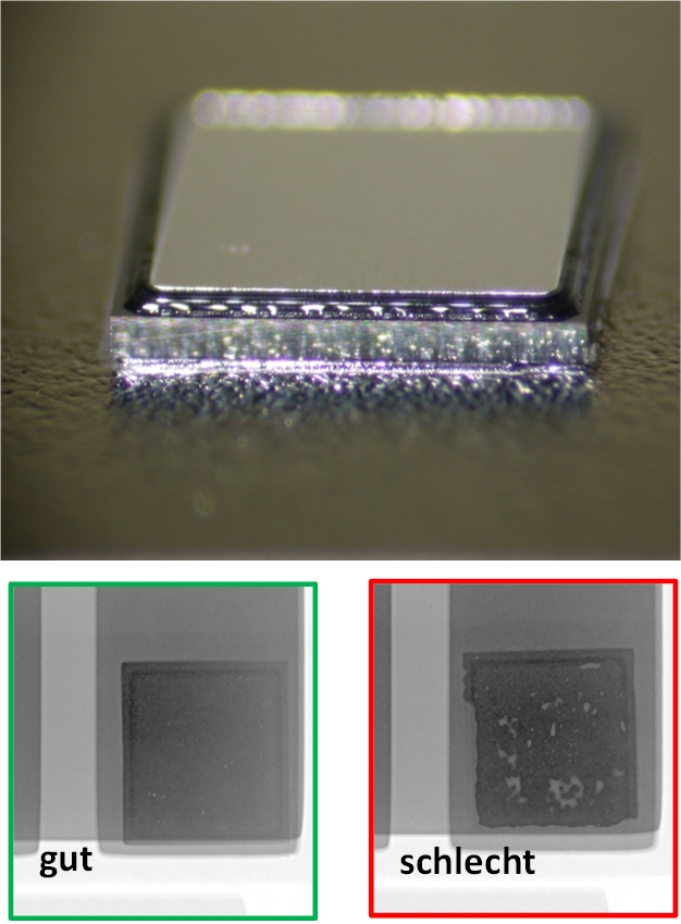 Fig. 4 Soldering resultsTheprocess activation or reduction of potentially present oxides on the surfaces is carried out by using activation gases such as forming gas (N2H2), formic acid (HCOOH) or pure hydrogen (H2), which are used in a sequence of purging processes. In addition, the residual oxygen is removed from the chamber and the residues of outgassing from the materials are removed as well as possible using a vacuum. The solder is then heated further and when the melting temperature of the solder in the peak zone of the solder profile is reached, the solder begins to flow and wets the metal surfaces of the substrate and the back of the chip. This process is supported by the further use of the activation gases, which promote the wetting process. Finally, the chamber is repeatedly placed under vacuum to remove any gas bubbles that may be present in the molten solder due to air inclusions or outgassing of the materials.
Vacuum-brazed connections of chip assemblies offer several advantages compared to the use of electrically conductive adhesives as connection material. Increased thermal conductivity (up to 60-70W/mK), better reliability, high cleanliness and low outgassing behavior are some of the most important advantages and make vacuum brazing particularly interesting for applications in hermetic housings. This is why this chip bonding process is preferred in the aerospace industry and for industrial high-power applications.
c) Sintering
Another method of assembling chips is silver sintering. A general distinction is made between the use of sinter pastes or prefabricated sinter foils and between sintering with or without pressure. At Cicor in Radeberg, sinter pastes are mainly used for pressureless sintering in the assembly process. This process is comparable to the assembly process with adhesives when applying the pastes by dispensing, loading the chips and the subsequent sintering process in a batch oven (sintering temperatures are in the range of 175°C - 200°C) and can be realized quite easily. Compared to electrically conductive adhesives, these sinter pastes are characterized by a higher reliability and a significantly better thermal conductivity of up to 140W/mK and are therefore particularly suitable for high-power applications.
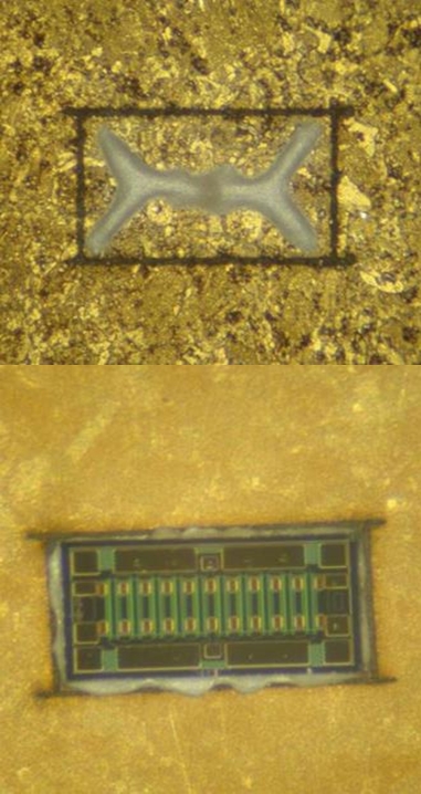 Fig.5 Example of sintering process forultra-thin chips
Ultra-thin chips with a minimum thickness of 20µm are preferred for applications where space saving is an important requirement (e.g. for medical applications). The assembly of ultra-thin chips is a challenging area of chip bonding technology, as these chips are very sensitive to damage. The pick-up process from the wafer, handling in the system through to placement on the substrate is critical. The warping of thin chips is an important parameter that must be controlled during the placement process and adhesive curing in the oven in order to achieve consistently good results. Cicor uses specially adapted, low-viscosity, electrically non-conductive adhesives. It is important to ensure good wetting of the adhesive on the chip and at the same time minimize the risk of contamination of the top of the chip. Picking thin chips from the wafer foil is a critical step as the thin chips are very fragile. This pickup process was evaluated and successfully tested for chip sizes up to 5mm x 5mm.
The pattern for the adhesive application was optimized to achieve a controlled flow of the adhesive by using the capillary effect and thus a controlled wetting on the chip. The adhesive does not wet beyond the chip edges to the top of the chip, so that no adhesive contamination occurs on the top of the chip. Samples for medical catheter applications (see Fig. 6) were successfully produced with 30µm thin chips. These were mounted on a polyimide film using the adapted chipbond process, then contacted and embedded. The flexibility of the structure in conjunction with the thin, space-saving chips enables them to be rolled up and inserted into narrow catheter housings, for example.
Summary
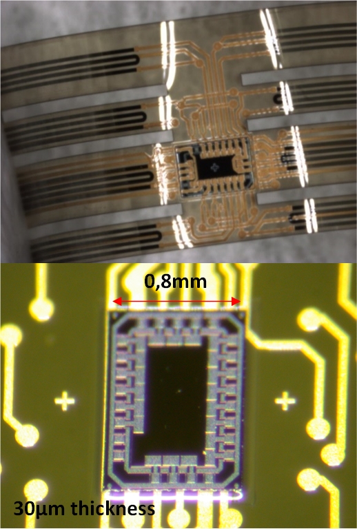 Fig. 6: Example chip with 30µm thicknessInthis article, various manual and automated chip assembly options such as bonding, vacuum soldering and sintering at Cicor, as well as their particular challenges and influencing parameters, were briefly presented.
Good results in chip bonding require a well-coordinated interplay of important criteria. Material quality, cleanliness and suitability for chip bonding processes, technical parameters such as placement accuracy, forces, temperatures as well as the selection of bonding materials and their application methods and much more also play an important role with regard to further processing in subsequent processes for the electrical contacting and encapsulation of chip assemblies.
For the successful processing of optical chips, for example, better clean room classes and well-trained and qualified employees are available. A wide variety of geometries, e.g. very small or very thin chips, can now also be processed automatically at Cicor in Radeberg in order to meet a wide range of miniaturization requirements in the industrial, medical technology and aerospace sectors. A range of very well adapted processes and systems for chip bonding are available for this purpose. In addition, new materials are constantly being tested and process adaptations developed in order to be able to offer successful solutions for constantly changing product and customer requirements.
