For 15 years, experts from the field of electronics production have been regularly 'going down into the depths' together with users. Initially with actual mine visits, over the years only in the figurative sense in the form of very well-founded lectures. After being canceled in 2020, the traditional event took place again at the end of September 2021 - for the first time in Leipzig.
 After last year's cancellation due to the pandemic, there was great joy that the event 'Wir gehen in die Tiefe' could take place again in 2021. As usual, current topics were discussed in depth and an outlook on future developments was provided.
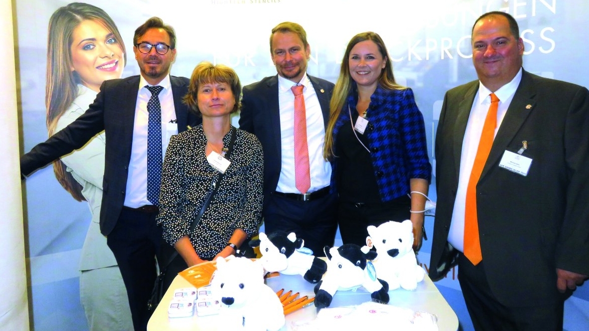
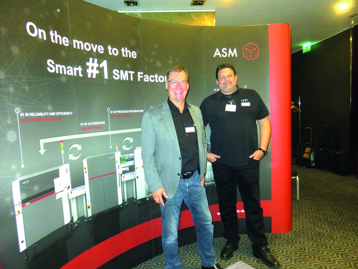
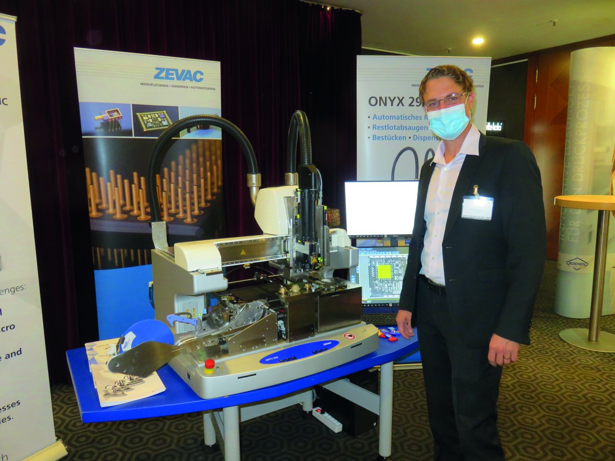
As in previous years, the event with a total of twelve presentations was organized by Thorsten Schmidthausen, 2ndMax GmbH, together with the partner companies ASM Assembly Systems GmbH & Co KG, ASYS Automatisierungssysteme GmbH, Christian Koenen GmbH, Heraeus Deutschland GmbH & Co KG, Rehm Thermal Systems GmbH, Vliesstoff Kasper GmbH and Zevac AG Deutschland. These companies also took part in the accompanying exhibition. The presentations were moderated by Prof. Dr. Mathias Nowottnick, University of Rostock.
Challenges during assembly
In the first presentation, Norbert Heilmann, ASM Assembly Systems GmbH & Co. KG, explained the challenges in assembly due to new trends in AVT. Developments in electronics mean that the range of components that need to be processed is becoming ever larger and more diverse. As a result of power electronics, large, heavier and THT components are increasingly being used. At the same time, miniaturization in SMT is continuing with even smaller passive components and chips. In order to be able to process all of this, assembly machines require even more powerful sensors and smart algorithms. High-resolution cameras and large fields of view are becoming increasingly important for detecting faults or damaged components before assembly. Checking that all components have been correctly assembled before soldering is becoming increasingly important. For the assembly of complex components or the placement of complex assemblies, special placement processes are required, such as sequencing, different placement levels and fiducial evaluation for different objectives. For example, LED and lidar components are aligned with their light-emitting surface according to slotted holes and drilled holes or notches, while the other components are aligned according to the etched copper marks. The aim of the further developments is to be able to assemble both SMT and THT components of all designs as fully automatically as possible.
 Prof. Dr. Mathias Nowottnick at the opening ceremony
 Thorsten Schmidthausen during the welcome address
 Norbert Heilmann
 Gianfranco Sinsitra
 Dr. Kai Kammers
 Michael Zahn
Smart factory based on standardized interfaces
Dr. Kai Kammers, Asys GmbH, discussed the question: 'Plug&Play Smart Factory through standardized data interfaces - wish or reality?' He first discussed the development of data interfaces and the corresponding standards for factory automation. He then made it clear that standardization and standardized solutions are only the prerequisite for the implementation of smart factories. This is because they naturally lag behind development and bring everyone up to the same level. They are a (starting) basis. But smart demands more. That is why continuous improvement (practiced by the company itself) is also necessary for the smart factory of tomorrow.
 Maximilian Barth
 Torsten Vegelahn
 Tobias Traurig
Protection of electronic assemblies
In his presentation on dispensing and coating to protect electronic assemblies, Gianfranco Sinsitra, Rehm GmbH, first listed the reasons for protecting sensitive electronic assemblies in many applications. Without a protective coating, there is an increased risk of dendrite growth and thus electronic failure in combinations of small conductor spacing, residues and moisture. However, protective coating also has its pitfalls, such as possible blistering, pinholes, delamination, cracking, dewetting and orange peel formation, as well as edge alignment and paint spatter. Gianfranco Sinsitra explained these and the advantages of prior cleaning before using his company's products to show what solutions are available today and how perfect coating management and reliable processes can be achieved.
 Prof. Dr. Norbert Willenbacher
 Oliver Albrecht
Paste printing on different levels
Even on non-planar surfaces, high-precision material deposits can be applied quickly and repeatably by printing in volume and position. Michael Zahn, Christian Koenen GmbH, explained how precision printing can be carried out on uneven surfaces. Using examples from customer projects, the solutions developed for printing over elevations and for printing in cavities (up to 2 mm deep) were described. Specially designed printing stencils (e.g. stepped stencils) and slotted doctor blades are used for this purpose. Customized printing parameters are also required. Christian Koenen GmbH develops not only the required printing tools but also the complete printing process.
 Thomas Liebscher
 Joey Kelly
Reliable spatial electronics
After the lunch break, Maximilian Barth, Hahn-Schickard-Gesellschaft für angewandte Forschung e. V., gave an overview of assembly and connection techniques for reliable spatial electronics. Starting with the special features of solder paste application and the assembly of three-dimensional substrates, he highlighted the problems and presented a roll-to-roll line for MIDs, among other things. The variety of possible materials and processes for spatial electronics requires a great deal of experience in material selection and design. Reliability can be influenced by varying the connection geometries. The reliability of spatial electronics is predicted using simulations and service life models based on reliability tests, whereby the simulations require precise knowledge of the geometries and connection points. Maximilian Barth concluded by providing information on his institute's previous work on reliability and lifetime modeling for MIDs.
 Speakers on the first day
Printers in the autonomous factory
 Torsten Vegelahn, EKRA Automatisierungssystem GmbH, outlined the challenges facing printers in the autonomous factory, i.e. what needs to be considered in order to successfully operate the printing process in the autonomous factory. There are several levels to get from the current state, where nothing works without an operator setting up the machine, to this point:
- Level 1: The autonomous machine performs the actual setup change independently, without an operator. The operator prepares the machine(s) during production.
- Level 2: In the autonomous line, an autonomous system (APA: Autonomous Process Assist) also supplies and removes the materials and tools (feeding the system). A person is required to prepare and process the materials and tools at a central location.
- Level 3: In the autonomous factory, the material flow and the process chain are fully automated: Materials, tools, components etc. are delivered and autonomously processed into the end product in the factory. Humans only monitor the factory.
Torsten Vegelahn used a modern Ekra printer to describe how the printing system can be transformed for the autonomy level and what properties are required from the printer. He also discussed standardization and safety aspects. To control the material flow, the smart factory requires a comprehensive solution based on the import of order and master data from the ERP/MES system, such as that offered by the Pulse Pro software from Asys.
Digital transformation
 Tobias Traurig, Zollner Elektronik AG, kicked off the second day of presentations by talking about the digital transformation in his company's production planning. Manufacturing companies have to face increasing challenges in order to remain competitive. For example, production is confronted with quantity and product changes on an almost daily basis. Digitalization is therefore also the order of the day here and is now one of the company's top projects. This is because all products and processes are affected. At the heart of this is the digital twin. The entire product life cycle is being digitalized. Tobias Traurig explained Zollner AG's digital production concept and, in particular, how this is being implemented in production planning. He noted that there is no digitalization without a PLM system.
 Speakers on the second day
Surface cleaning using electrostatic discharge
 After Thomas Liebscher, Kist & Escherich GmbH, had explained the basics of surface cleaning using electrostatic discharge, he used numerous application examples to illustrate where this is used today and which systems and devices his company offers for this purpose. The variety is impressive. These include electronics applications such as the cleaning of printed circuit boards. The challenge here is that the PCBs can easily become electrostatically charged, which must be avoided. After depaneling, loose particles and dust often adhere to the surface. Both are possible sources of functional impairment. The cleaning solution from Kist & Escherich is the Taifun-Clean cleaning system, which is installed above the conveyor section in the production line. The integrated ionizing bars remove electrostatic charges from the circuit board and the pulsating compressed air vortex generated by the device removes the particles from the surface. The contaminated air is also extracted.
New materials based on capillary suspensions
New materials for flexible, printed electronics based on capillary suspensions were presented by Prof. Dr. Norbert Willenbacher, Karlsruhe Institute of Technology (KIT), after he had explained the phenomenon of capillary suspensions. Capillary forces of a second, immiscible liquid can significantly change the properties of suspensions, such as the transition from liquid-like to gel-like behavior or from weak to strong gel. The effect also occurs if the liquid wets the particles less well than the main liquid. These effects were illustrated using the example of CaCO3 particles suspended in varying proportions (0 to 0.5 %) in an organic solvent. Prof. Dr. Norbert Willenbacher then explained how such new materials can be produced and where they are already being used. They are used, for example, as pre-materials for porous sintered materials (ceramics, glass), in silver pastes without non-volatile additives and for printed and flexible electronics, where they induce the formation of conductive structures with their capillary forces, which was illustrated using a number of application examples, including sensors and electrical connections.
Limit values for the coplanarity of components and substrates
 During soldering and operation, temperature changes cause both components and substrates to bend due to different thermal expansion coefficients. Possible consequences include the head-in-pillow effect in BGAs, solder bridges and pad tears, and stresses arise in the solder joints that are characterized by the different deformation behavior of the assembly partners. This was investigated in the AiF-funded Warpage_ZUV project. Oliver Albrecht, Dresden University of Technology, presented the results in his lecture "Bending of components and substrates - influences on quality and reliability and suggestions for limit values". The general rule for the realization of reliable solder joints is that the coplanarity deviations of the components at the melting temperature of the solder should be smaller than the wet film thickness of the solder paste. Accordingly, the limit value recommendations for the coplanarity deviations are as follows:
- BGA: not greater than the wet film thickness regardless of size and pitch
- LGA: 25 % of the wet film thickness
- QFP: 75 % of the wet film thickness
- QFN: 50 % of the wet film thickness
- DCB: no recommendation, as there are too many variations
- LP: no recommendation, as available data classifies PCBs as uncritical
Good wettability increases the limit values. Convex bending is more favorable. The coplanarity at room temperature should not be zero and should be remeasured for large components and critical applications.
How 'No Limit' works
 After lunch, Joey Kelly gave a keynote speech entitled 'No Limits' about his eventful life as an athlete, musician and manager of the Kelly Family. Using many photos, he described the achievements - including 8 Ironman participations in one year - which he tackled and overcame with the motto 'You have to set yourself a goal and then you just have to start': "If there is a setback, just keep going. After all, life is a marathon."
Safety and risks of technology
In the closing lecture 'No Risk no Fun - Safety and Risks of Technology', Prof. Dr. Mathias Nowottnick, University of Rostock, used examples from everyday life to illustrate the problem that small causes often have a big impact. For example, broken solder connections have already had catastrophic consequences, such as the crash of an A320 over the Java Sea in 2014. Prof. Dr. Mathias Nowottnick explained the terms quality: error, tolerance, defect, reliability and failure rate. He emphasized that the largest possible number of identical products must be examined in order to reliably determine failure rates and that risks can only be calculated if all influencing factors are known. Using the example of power plant technologies, he showed how economic risks can be compared with each other in terms of the extent of damage and probability. However, not all risks can be assessed economically (e.g. in medicine) and statistical statements can only be compared if they have the same reference basis. He used a nonsensical correlation between tax fraud and life expectancy to illustrate that a statistical correlation says nothing about cause and effect.
The lecture and supporting program therefore offered a lot and 'We go into depth' was implemented again.
