")
")
")
Plasmatreat GmbH, a global leader in the development and manufacture of atmospheric pressure plasma systems and equipment, covers all production steps in semiconductor and electronics manufacturing with its solution portfolio - from front-end to back-end, leadframe treatment to PCB production, assembly and conformal coating.
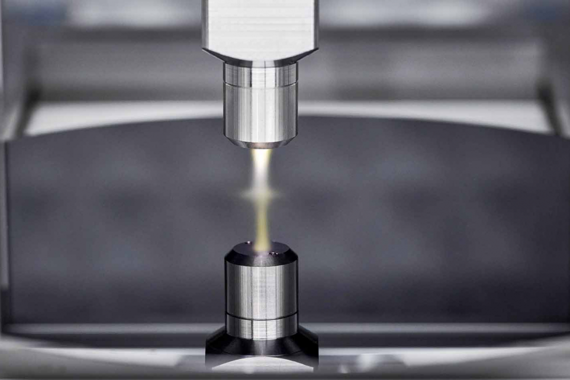
The plasma technologies ensure reproducible, efficient processes, improved adhesion and greater reliability and durability. The focus is on processes for flux removal and rapid oxide reduction. Potential-free plasma is used to reliably remove organic and inorganic residues, activate surfaces in a targeted manner and reduce oxides inline.
World premiere - new nozzles especially for semiconductor production
The new PBD100 DBD nozzle is suitable for flat, atmospheric plasma applications with a treatment width of up to 100 mm. It enables uniform, large-area activation of sensitive substrates and removes organic residues and oxides without particles - with high process stability. The PFA10 is a low-particle, potential-free nozzle for precise local treatment. It removes organic residues and oxide layers, activates metallic and polymer surfaces and thus creates optimum conditions for hybrid bonding and chiplet stacking.
productronica: Hall A2, Stand 445
SEMICON Europe: Hall/Stand B1136
![]()
Plasmatreat GmbH
Queller Str. 76-80
33803 Steinhagen
Phone +49 5204 9960 0
m
