Semiconductors are needed in practically all areas of our lives. From consumer electronics to automotive electronics, medical technology and defense technology, there is practically no area of life in which semiconductors are not part of the 'electronic brain'. The fact that this market is expected to have a volume of 1 trillion $ = 1,000 billion in 2030 illustrates the dimensions(Fig. 1).
") Fig. 1: Global semiconductor market forecast 2019 to 2030 (data: WSTS/TMRC)
Fig. 1: Global semiconductor market forecast 2019 to 2030 (data: WSTS/TMRC)
Demand for semiconductors will virtually double from today's USD 526 billion by the end of the decade. Nobody knows today what share artificial intelligence (AI) will have, but the fact is that AI is an accelerator for the demand for high-performance chips.
AI as a game changer
The expected share of 40% HPC (High-Performance Computing) is as large as mobile and IOT (Internet of Things) combined(Fig. 2) This was not thought possible just a few years ago. The launch of Chat GPT less than two years ago was a game changer. It is also known as the 'iPhone moment' for artificial intelligence (AI).
") Fig. 2: Semiconductor market 2030 forecast by application (Data: TSMC/IEEE)
Fig. 2: Semiconductor market 2030 forecast by application (Data: TSMC/IEEE)
The triumph of the foundries
By outsourcing the highly complex semiconductor technology development and wafer production from the IDM model, the newly created foundries were able to focus on their core competencies. This led to a considerable acceleration in chip development. This explains TSMC's current technological leadership as the world's largest foundry ahead of INTEL, the long-time IDM leader.
In addition to the foundries, other new business models such as fabless chip manufacturers and system houses have emerged.
While integrated device manufacturers (IDMs) such as Intel still dominated in 1990 with a 75% share of global chip sales excluding memories, their share had fallen to 55% by 2010(Fig. 3). According to a forecast by TSMC and the IEEE, IDMs will only account for 30% of sales in 2030. In contrast, fabless manufacturers such as Nvidia, AMD and Qualcom have begun their triumphal march with the rise of foundries. After a 2% share of sales in 1990, fabless manufacturers already accounted for 23% in 2010. According to forecasts, this is set to rise to 40% of global chip sales in 2030, plus a 10% share of sales by system houses.
") Fig. 3: Foundries create growth for fabless and system houses (Data: TRMC)
Fig. 3: Foundries create growth for fabless and system houses (Data: TRMC)
Will cars be software-oriented or silicon-based in the future?
The future of the automotive industry is defined differently depending on the perspective. Some see the car of the future as a mobile computer that is software-oriented.
Bosch has developed a new IT platform that centralizes and processes all data as an ADAS integration platform(Fig. 4). The modular design of this small supercomputer not only saves costs, it also provides a high degree of flexibility for different brands and vehicle types. Due to the high level of integration possibilities of the central electronics, there are already plans to fully equip vehicles ex works in terms of hardware and software and to activate certain functions 'over the air'. In this way, manufacturers can create new sources of income through user fees.
Semiconductor manufacturers, who see automotive computers as a silicon-based technology, take a completely different view, as semi-autonomous or autonomous driving is not possible without the necessary semiconductors.
 Fig.4: The future of the semi-autonomous/autonomous car with extensive sensor technology evaluated in a central computer
Process development using the example of TMRC
Technologically, there have been several leaps in chip architecture. Until around 2014, the planar production method was used for 22 nm structures. From 2014 to 2024, the FinFET architecture was used for structures of up to 3 nm. From 2024, this is to be replaced by the nanosheet architecture, which currently maps structures down to 2 nm.
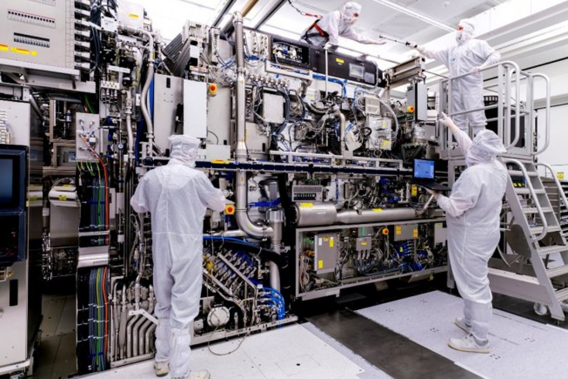
In addition to chip architecture, lithography technology plays a key role. From 2010 to 2019, immersion lithography dominated, in which ultraviolet radiation passes through a lens system via a thin liquid film onto the photoresist-coated wafer. Exposure structuring was further developed from single pattering for 28 nm nodes to double pattering with 22 nm nodes and self-aligned double pattering for 7 nm nodes. A significant leap forward began five years ago with the use of EUV lithography. The extreme ultraviolet lithography process uses electromagnetic waves with a wavelength of 13.5 nm(see article image above).
 Fig. 5: The process development using TMRC as an example
What happens next?
One of the main drivers of chip development is energy efficiency. This has improved by a factor of >80 from the N28 node in 2011 to the N3 node this year. This has also created a crucial prerequisite for AI applications, as the power consumption of data mining is accumulating.
The electricity consumption of data centers was estimated at 200 TWh in 2020, corresponding to 1% of global electricity consumption. This is also expected to increase to 3% by 2030 due to AI. The power consumption of high-performance computers (HPC) is therefore not negligible.
From 2025, 2 nm nodes are to be produced with the nanosheet transistor architecture. After that, the CFET architecture will be used for 1 nm structures. CFET is the abbreviation for 'complementary field-effect transistor'. These are folded N&P MOS transistors, which are intended to further reduce the space requirement.
Packaging technology for HPC and AI
Advanced packaging has become the holy grail of the semiconductor industry. After Flip Chip (FC) came System on Chip (SoC) and now Chip-on-Wafer-on-Substrate (CoWoS). The future trend is towards the monolithic block through 3D stacking in the system on integrated circuit (SoIC). This is the only way to further increase signal speeds and reduce energy consumption.
In a nutshell
- The semiconductor market, driven by HPC and AI, will grow from USD 526 billion in 2023 to USD 1,000 billion = 1 trillion by 2030
- According to a forecast by foundry world market leader TMRC, HPC will have a 40% share by 2030, mobile 30% and automotive 15%. IoT, on the other hand, is only expected to have a 10% share, in line with previous expectations
- By outsourcing chip process development and wafer production to the foundry business model, IDMs such as Intel have massively lost importance. These market shares have been taken over by fabless manufacturers and system houses
- New chip processes such as nanosheet transistor architecture for 2 nm nodes and CFET architecture for 1 nm structures are about to be introduced
The importance of semiconductors for global economic output (GDP) is illustrated by the following data: in 2030, foundries are expected to account for a global share of GDP of USD 250 billion, the semiconductor industry USD 1 trillion = USD 1,000 billion and the electronics industry USD 3 trillion. The IT industry, including AI, generates a gross value added of $11 trillion.
Semiconductor and packaging technologies are advancing rapidly, and with them applications for future markets. Japan and South Korea have recognized this and are making huge efforts to keep up, while the USA is trying to make Intel the technology leader again.
I wish you a productive springtime.
 With best regards
Yours
Hans-Joachim Friedrichkeit
