Under the motto 'Fast, faster - high speed', tasks in PCB and assembly design were discussed. The focus was on the topics of high speed and impedance control. Guided tours of the Research & Innovation Center and Würth Elektronik's PCB production facilities rounded off the 12th PCB Designers' Day organized by the FED.
 Reinhold Würth University of Applied Sciences in Künzelsau
Pursuing the realization of your own design
With 'My design in production', participants at the 12th PCB Designers' Day were given the opportunity for the first time to submit design data and see their own design live in production. The key data required for this was made available to interested parties in advance for downloading. The design was integrated into a panel. The production process could be followed during the factory tour at Würth in Niedernhall. At the end, the participants received the printed circuit board produced with their design.
High-speed and impedance laboratory - tour and demo
The Designer Day began the afternoon of the previous day with a visit to the Research & Innovation Center at Reinhold Würth University of Applied Sciences in Künzelsau. There, the high-speed and impedance laboratory was visited in small groups and the theory on which the measurement technology presented was based was explained in short presentations.
Hermann Reischer, Polar Instruments GmbH, Nussdorf am Attersee, Austria, presented the new ATLAS VNA attenuation measurement system for printed circuit boards. It has been specially developed to provide PCB manufacturers with accurate and repeatable measurements of intrinsic attenuation according to Delta-L 4.0 in the production environment. The system consists of the ATLAS VNA software, the Anritsu ShockLine MS46524B vector network analyzer as well as the required precision cables and special test probes for safe contacting of the test specimen. The Delta-L test method is compliant with IPC TM650 2.5.5.12 and uses the comparison between a short and a long cable. Hermann Reischer explained the special features and the measurement procedure with the system. In addition to the attenuation of signals with frequencies of up to 43 GHz, it can be used to measure the intrinsic value uncertainty, the S21 parameters of the cables, the phase response and the effective permittivity of the test specimens. Würth Elektronik has the only ATLAS VNA system in Europe. This is also offered as a new service for measurements for third parties.
Andreas Dreher, Würth Elektronik, explained on "HIGH.speed: Design for Manufacturing" how the various materials differ in HF/HS applications. For very high frequencies or very fast signal rise times, Megtron 6 is more suitable than conventional materials (FR4). In addition, the layout and the layer structure are important factors influencing the conductor properties, as these influence the local current density and thus the resulting copper thickness during the conductor pattern structure. For this reason, an even copper distribution on the layers should be aimed for and critical signals should be placed on the inner layers.
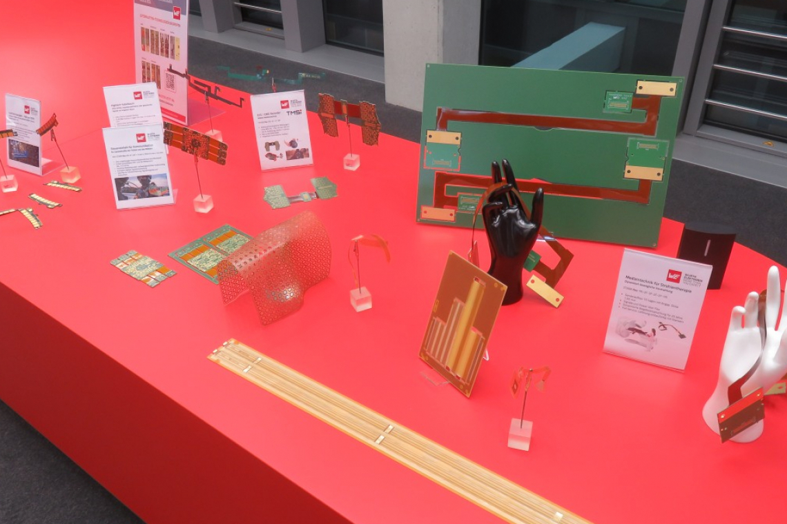
Michael Matthes, Würth Elektronik, provided information about the 'WEdesign' layout service. The service offered by Würth Elektronik starts with the circuit diagram or just the parts and net list and offers extensive resources for quick solutions in bottleneck situations. There are currently around 60 layouters working for WE in India, which has been serving the Indian market since 2014. Layouters/designers and AV/CAM have direct contact and can coordinate closely on questions, which is very important in the HS and HF sector. By using known and proven technologies and layer structures, the reliability and quality of the PCBs and assemblies increase and improved tolerances can be achieved. Production-optimized layout creation based on WE design rules is carried out for all common technologies (multilayer, rigid-flex, high-speed, high-power, HF, etc.). The EDA tools Allegro/OrCAD, Altium Designer, Siemens (Mentor) Xpedition, PADS Standard Plus and Professional are used for this purpose. Accompanying analyses and simulations are carried out with HyperLynx SI/PI/Thermal, Ansys Icepak and the Polar tools SI9000e-Speedstack, Quicksolver and Coupon Generator. Mechanical design with Solidworks is also offered, which was illustrated using examples. The design possibilities of the EDA tools were demonstrated using additive solder resist masks with several height levels and meander-shaped conductor structures for stretchable substrates.
 Andreas Dreher talked about the materials
 Hermann Reischer presented the new Delta-L 4.0 measuring process
 Michael Matthes provided information about the 'WEdesign' layout service
During the breaks, the exhibition in the showroom could be used for networking. This was followed by a guided tour of Würth Elektronik's PCB production facility in Niedernhall. In line with the production process sequence, the lines from inner layer production to final inspection were visited one after the other, with the quality assurance measures and tests being explained in each case. There was also a demonstration of the application of the digital solder mask with an inkjet system and a look at the control station.
The current situation of the entire production is visualized online on the control station so that everything can be monitored and controlled on the basis of this data. To this end, those responsible meet there twice a day for around a quarter of an hour to coordinate their activities. In addition, there are so-called QOOL info monitors on all lines, on which the respective key figures and other data, including the 6S status, are displayed online so that everyone is informed.
 Würth Elektronik's printed circuit board plant in Niedernhall
Further information from the factory tour was that WE applies ENIG as the only final surface in the factory and that the programs for the electrical test systems are created in India. As the cost of creating and maintaining test adapters is very high and the quantities are getting smaller and smaller due to technical developments, WE has decided to only use finger testers and to phase out the other systems, i.e. the parallel testers. Further investments in finger testers are planned.
Several participants had the opportunity to visit a PCB plant for the first time and were very impressed by the number and size of the systems.
Later on, the business dinner was used for intensive networking and exchanges between the experts. There were still a number of detailed questions to be clarified in small groups.
Topics ranged from CAM, the HS guidelines and HS design practice to LP for GHz applications
The next day started with the official opening of the 12th PCB Designer Day. FED board member Erika Reel welcomed the more than one hundred participants and thanked the host Würth Elektronik for the good cooperation. Daniel Klein, Managing Director of WE-CBT, then welcomed the guests. He thanked the FED for the good cooperation and provided information about the Hohenlohe region. FED Advisory Board member Markus Biener, Zollner Elektronik, then took over the moderation. He gave a brief overview of the FED's range of services and talked about the PCB Design Award, for which applications can be submitted until the end of May. This was followed by the technical presentations.
 Erika Reel during the welcome address
 Daniel Klein also used the welcome address to provide information about the Hohenlohe region
 Markus Biener moderated the presentations
Worlds come together
Matthias Hohenstein, Würth Elektronik, Team Leader CAM, described the situation based on the top-stop reasons and the data formats and looked at the consequences of the different data specifications and interpretations of aspect ratios, small BGA grid dimensions, soldering areas on BGA pads, impedance structures, back-drilling, open DK drill holes, rigid-flex transition and homogeneous copper distribution as well as markings. Stops in CAM processing can be avoided by adhering to design rules and clear and unambiguous specifications. Clarifications in advance are also helpful. Matthias Hohenstein explained what WE prefers and how WE implements the specifications as standard. He asked that the parameters be transferred to manufacturer-specific design rules after clarification in order to avoid constant queries. Observing these points and the design rules/design guides for the LP technologies offered by WE, which can be found on the website www.we-online.com, supports faster processing, adherence to the agreed delivery time and quality assurance - a win-win situation for everyone.
New FED High-Speed Guide
Rainer Thüringer, TH-Mittelhessen, presented the new guide, which was created by professionals for beginners in the FED High-Speed Working Group. It is intended to make it easier for PCB designers and layouters with a few years of professional experience to get started with high-speed designs. The guide was originally planned for publication in the FED series Band des Wissens (BdW). However, it is now to be made available online shortly so that it can be used in parallel with day-to-day business, complementing the FED three-day seminar on high-speed design. On a total of 90 pages, technical terms and special features are explained and the necessary layout measures are presented and explained using examples:
- What needs to be considered in advance?
- What type of PCB is required?
- How are HS signals transmitted?
- What needs to be taken into account, e.g. for plug connections?
Among other things, the following features of impedance-controlled multilayers are discussed:
- Layer structure and microstrip/stripline
- Return current path, cable routing and termination
- Bus wiring/topologies (equal lengths of differential lines, meander shapes, loose/fixed coupling)
- Pulse power supply (PDN) with potential layer pairs and capacitors
- Shielding layers and crosstalk
- Signal attenuation, tan delta and material selection
Rainer Thüringer used examples to illustrate the content and described the underlying physics of electromagnetic wave propagation by comparing it to water waves. The guide also discusses concurrent driven design and high-speed tools.
 Matthias Hohenstein explained what needs to be considered for CAM
 Rainer Thüringer presented the new FED High-Speed Guide
 Georg Scheuermann looked at high-speed design in practice
High-speed design in practice
Georg Scheuermann, TQ-Systems, showed what challenges high-speed design brings with it in practice and used numerous examples to explain how to successfully meet the requirements on the PCB. He addressed the following points:
- Signal attenuation and choice of PCB material
- Avoidance of impedance jumps
- Minimization of stub lengths on vias
- Length adjustment DDR
- Reference layer change
- Length adjustment of differential signals taking into account the minimum distance (clearance) to avoid etching problems
- Optimization of the pin assignment, as fast signals should always have a GND pin next to them
- Impedance calculations.
For example, the attenuation for 100 Gbit Ethernet signals from the processor to the SFP connector must not exceed 7.3 dB. This loss budget includes the attenuation of the circuit diagram on the PCB (vias, conductor structures) and the attenuation of the connectors. In order to provide as much loss budget as possible, the low-loss material Megtron 6 was chosen for a base board. In addition, impedance jumps must be avoided in the design. This can be achieved, for example, by leaving reference sensors free under the components, for which the rule of thumb is that leaving them free is recommended if the component pads are significantly wider than the conductors.
The new Delta-L 4.0 measurement method for material qualification
Hermann Reischer, Polar Instruments, provided information on PCBs for GHz applications and presented the new Delta-L 4.0 measurement method for material qualification. Increasingly sophisticated designs and transmission frequencies in the GHz range require precise knowledge of PCB material properties. At frequencies above 3 GHz, it must be taken into account that the lines on the PCB are lossy, i.e. the impedance must be defined and the maximum attenuation must be controlled. The attenuation depends on the cable length and cross-section, the loss factor tan delta of the base material and the copper roughness. The dielectric losses and copper roughness have a significant influence on signal integrity. Hermann Reischer explained the formula for the impedance of the lossy transmission line. With the new Delta-L 4.0 measurement method, the PCB industry now has a production-ready test method for qualifying materials up to 43 GHz. It is based on the Intel Delta-L method. A vector network analyzer (VNA) and special probes for coupon contacting are used for measurement. Hermann Reischer explained the special features, including the specially designed footprint for measurement and de-embedding via line length difference. This involves first measuring a long section of cable with a defined length and then measuring a short section of cable with a defined length.
In the afternoon, the event concluded with a guided tour of Würth Elektronik's modern PCB production facility in Niedernhall and a meeting of 'My design in production'.
 Speakers at the 12th PCB Designer Day
