
Numerous questions arise regarding the construction of pure flex PCBs - especially when it comes to plated-through holes using button plating. What exactly is this and why is this technology needed?
If we first look at the basics of producing a rigid PCB, the inner layer cores are structured at the beginning of the process (exposure, etching, etc.); then - after pressing the cores with prepreg and drilling - the first copper build-up takes place with through-hole plating, followed by full-surface plating (panel plating) with electrolytically deposited copper (ED copper, electro-deposited). Finally, there is the electroplating of the conductor pattern (pattern plating). This sequence results in a structure of three copper layers on a copper foil. The production process for a flexible printed circuit board differs from this, as each additional copper layer counteracts the flexibility, so no additional copper layers are required on the base copper.
In order to achieve a flexible structure, RA copper (roll anneal copper) is used as the base copper for flex PCBs. RA copper is rolled from copper ingots and has a high ductility. Electrolytically deposited ED copper is also used in further construction. It has a more granular structure. If flexible printed circuit boards such as a conventional multilayer printed circuit board are coated with ED copper, different copper layers with different structures and flexibility are obtained. Button plating offers a solution for adapting the manufacturing process so that the different properties of RA and ED copper can be managed. With button plating, only certain areas of the conductor pattern of a purely flexible PCB are reinforced with ED copper, preferably areas with vias and solder/support pads.
For this purpose, the areas that are not to receive a copper coating are selectively masked during the production process. This also explains the term button plating. If you imagine a purely flexible PCB in cross-section, you would see a flat surface from which some areas protrude like buttons.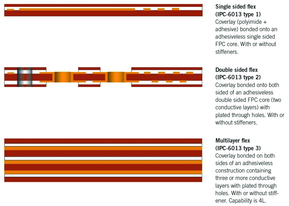 Flex types according to IPC-6013
Smaller line widths and spacing possible
An additional advantage of button plating is the possibility to realize smaller line widths and distances. Increasing miniaturization often requires flex PCBs to be developed for smaller installation spaces. However, pure flex PCBs that are almost 60 cm long have already been manufactured. In the conductor pattern of a normal multilayer, almost all outer structures are coated with copper. As this coating is 3-dimensional (top, bottom, side), the distance to all structures is reduced.
When using button plating, the circuit of the purely flexible PCB is ready as soon as it has been structured and etched. Since with button plating only the area to be reinforced is coated with copper, the conductor spacing is not reduced and finer structures can be realized.
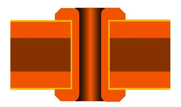 Cross-section of flex PCB with through-hole platingExample: If you are limited to around 75 μm line, width and spacing with a multilayer PCB, around 50 μm can be achieved with a fully flexible PCB. This 25 μm difference can make a big difference, depending on the design. The design can become more compact, which supports miniaturization and the ability to have smaller structures closer together.
Only 25m2 less, but a big difference
Conclusion: Rigid and flexible PCBs often use different materials and employ different techniques and production processes. It is important to know this in order to be able to take the PCB manufacturing processes into account during the design and procurement phases. If you have just started working with flexible PCBs, you may need a different manufacturer for your flex PCBs than your previous multilayer PCB supplier. The NCAB Group can offer a high mix of different technologies and support, both in design and in choosing the right factory.
