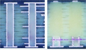
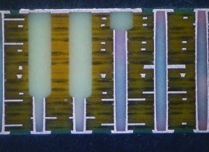
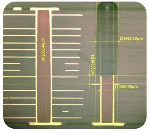
Kinwong, one of the world's largest PCB manufacturers (3rd place in China), is investing heavily in the development and production capability of HF PCBs with a high number of layers.
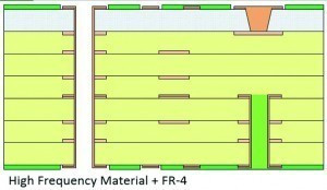 With a low number of layers, HF is now easily manageable. However, as the number of layers increases, it becomes increasingly challengingInthe age of 5G, new materials and approaches are not only required at chip and RF component level. The PCB must also be designed for high frequency and high speed. This also requires PCB manufacturing technology that is geared towards this. In particular, if you want to advance to a higher number of layers - and this is becoming increasingly necessary as requirements grow - the PCB manufacturer must develop and expand the corresponding capabilities through development activities.
Many electronic applications require ever higher frequencies. As the frequency increases, the scope for errors and/or deviations on the PCB decreases considerably. The use of high-frequency materials such as PTFE substrates, the use of blind vias or manufacturing parameters such as strictly controlled etching tolerances are required to make assemblies reliable for such high frequencies.
PCBs with a high number of layers (according to the definition ≥10L) are mainly used in communication devices, high-quality servers, medical instruments, industrial automation, aviation and military applications. These PCBs are subject to stricter requirements in terms of both the areas of application mentioned and the data streams/frequencies. Reliability is ensured by stricter registration and impedance control, which require more effort the more layers the PCB has.
Kinwong's Capability
Items | General capability | Advanced capability (HLC factory) |
Max. layers | 20 L | 24 L |
Max. working panel | 545 mm × 680 mm | 620 mm × 950 mm |
Max. board thickness | 3.2 mm | 5 mm |
Min. drill size | 8 mil | 6 mil |
Max. aspect ratio | 12:1 | 18:1 |
Registration | ±5 mil | ±3 mil |
Back drill stub | 6 mil ± 4 mil | 5 mil ±3 mil |
Impedance tolerance | ±8 % | ±5 % |
Insertion consistency | 0.05 dB/inch | 0.03 dB/inch |
Material | High frequency material, M2/M4/M6/M7 grade high speed material | |
Special workmanship | Hybrid Lam., POFV, small via back drill, skip via (L1-L3), step cavity, partial heavy copper, segmented gold finger, N+N structure, buried resistance, etc. | |
In addition, with 5G it is not only antennas that are increasingly integrated directly. More components also have to be accommodated in a smaller space. This requires multilayer PCB technology, whose processes, base materials and starting materials must be comprehensively considered and improved.
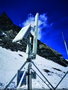 Thetransmission power of a 5G base station is greater than that of a 4G base station, and the corresponding requirements for the assemblies cannot be met with higher-quality materials alone. This also requires the system layout to consider and improve the properties with regard to high frequency, high speed and efficient thermal management.
Most important applications
- High-performance servers
- Switching centers Telecommunications and IT
- Mobile radio base stations
- Industrial control technology, control cabinet
- Power generation, distribution and storage
- Optical modules
Kinwong has now invested RMB 5 billion (€675 million) in the Zhuhai production site to establish the industry's leading PCB production facility for this sector. So far 40 layers have been achieved, the average number is currently 12 layers. HLC production supplies the communication, network, server, storage and security sectors. SLP production supplies PCBs with any number of layers, which are used in consumer electronics (e.g. cell phones, smart wearables, tablets, cameras, notebooks), IoT applications, industrial control systems and automotive electronics.


