Technologies to improve heat dissipation and high current management in printed circuit boards are constantly being developed to meet the requirements of increasingly complex applications.
The ALBA Group offers a range of technical solutions to meet the challenges of such applications. This is especially true when a digital part with very strict parameters (QFN microcomponents, BGA, layout with reduced conductor width and small electrical distances between the conductors themselves) is to be combined with a pure power part of the PCB that requires a copper thickness of more than 70 µm (e.g. up to 3 mm) in order to withstand high currents and complex thermal management.
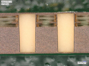
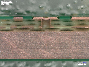
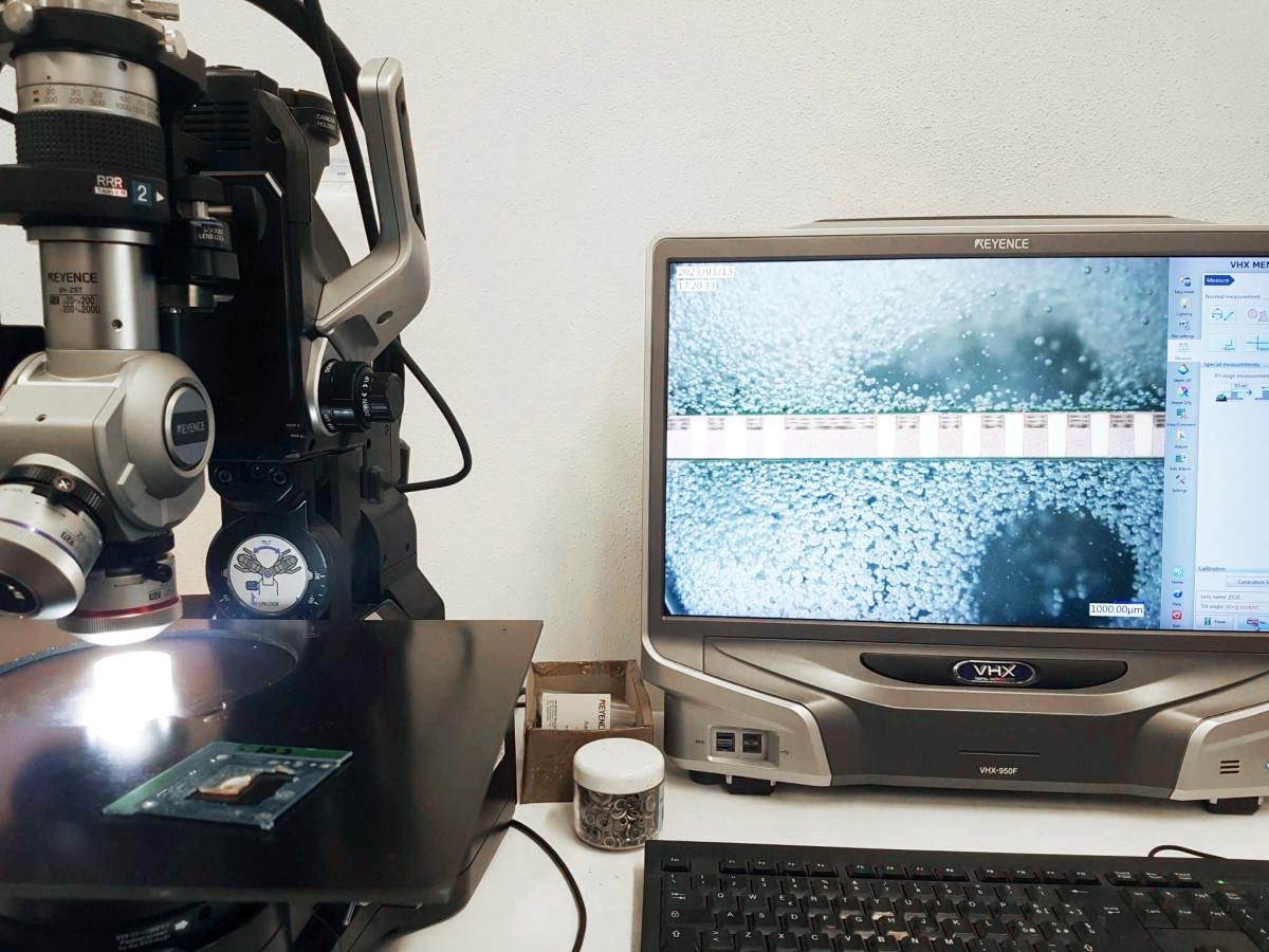 Fig. 2: Microscopic view of the micrograph
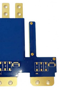
EBB printed circuit boards (embedded bus bars)
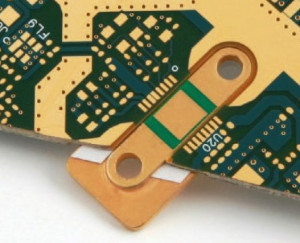
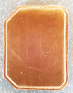 Fig. 3: Example of a copper core ('coin')PCBs with integrated bus bars have strips or bars of conductive material embedded in one or more layers of the PCB and can be manufactured in different shapes, thicknesses and sizes depending on the specific requirements of the project. They have the function of connecting different points of the circuit by managing very high currents without causing thermal overloads due to the Joule effect and without the need to take special precautions for the thermal management of the PCB.
This technical solution can also significantly reduce the overall size of electronic devices, as there is no need to install other external conductive elements. It is also possible to produce BusBars that protrude from the profile of the PCB so that they can be connected directly to a thick high-current metal wire via power connections.
EBB technology is used for a wide range of applications, such as power supply and charging systems for electric vehicles, DC/DC converters and LED lighting devices.
Embedded Copper Coin (ECC) PCBs
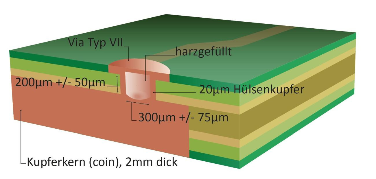
By taking advantage of embedded metal technology and taking into account that the thermal stress caused by the operation of printed circuit boards at high temperatures is one of the main causes of malfunction of power components, especially when they are manufactured with printed circuits with high integration density, it is possible to apply embedded metal inserts (copper) of considerable thickness (of the order of millimeters) on the printed circuit, positioned on the power dissipation areas of the power components: These inserts are generally referred to as 'coins': Components such as the MOSFET transistors can therefore be soldered directly onto these inserts, allowing easier thermal management than if a generic design of dissipative pad with or without thermal vias were used. The high temperatures reached by these power devices make it necessary for the PCBs that house them to ensure effective transfer and distribution of the thermal energy generated during their function, both to the ground planes of the PCB itself and to the external heat dissipation planes (which are then connected to additional heat sinks).
Printed circuits with these 'coins' therefore contain massive copper elements with small dimensions (typically equal to the power dissipation of the power component in question) and considerable thickness (even as thick as the PCB), which have the task of conducting heat through the circuit section. The shape of these inserts can be rectangular, but can also be shaped as required (e.g. for MOSFETs connected in parallel or in series). Their profile can have lips of different thicknesses to allow the passage of conductors that are not connected to them (highly digital design). They can also be mechanically processed so that they have a hollow surface compared to the surface of the printed circuit in which they are integrated.
This technology is often used to improve thermal management in designs where there are certain localized areas with elevated temperatures by integrating a heat sink into the PCB, but it can also be combined to increase the distributable electrical current within the PCB by combining the technology with integrated power rails. ECC circuits are often used in the automotive industry, medical technology and the new generation of telecommunications/data communication infrastructures, but also on high-performance PCBs in industry.
To summarize, the integration of 'busbars' or 'coins' in printed circuits represent advanced and innovative technological solutions that offer many advantages in terms of reliability, performance, footprint and overall cost of electronic devices compared to traditional PCBs.


