
Although the industry knew how to help itself with online formats, it still sorely missed the usual face-to-face events. This included the traditional SGO PCB seminar, which was canceled in 2020 and could not take place on the usual early summer date in 2021. It took place in September - with palpable joy at the genuine reunion.
Almost 80 participants from Switzerland, Austria and southern Germany were welcomed by Peter Weber, Chairman/Speaker of the PCB specialist group of the Swiss Society for Surface Technology (SGO SST), on September 22 in the conference hall of the Uediker-Huus in Uitikon near Zurich.

In-depth look at PCB manufacturers in Austria/Switzerland by technology and application focus
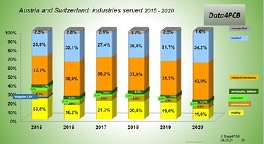
Before the technical presentations began, Remo Fischer (Hofstetter PCB AG, Küssnacht) gave a brief market analysis of Europe with a special focus on the DACH region. He primarily drew on the Data4PCB study by analyst Michael Gasch, also known as PLUS author, which describes the situation in the industry in Europe and Germany, Austria and Switzerland up to and including 2020. The long-term downward trend in the number of market providers is just as well known as the dip that followed a good 2018 in 2019 and (pandemic-intensified) 2020.
 Dr. Jakob Heier, EMPA
 Dr. Rodica Ababei, GS Swiss PCB AG
 Jürgen Haungs, Schmid Group
Fischer looked in detail at the situation in Switzerland and Austria before concluding by showing the forecast figures for 2021: Europe is expected to almost reach the PCB sales of 2018 with just under USD 2.27 billion (2019: 2.09 billion and 2020: 1.95 billion). For PCB manufacturers based in North America, sales of USD 3.4 billion are expected for 2021. In previous years, this figure was 3.16 billion in 2018 and - what was felt as a dip in Europe only had the character of a plateau on the other side of the Atlantic - 3.22 billion in 2019 and 3.20 billion in 2020.
A look at Asia reveals completely different figures: The 2019/2020 dip was noticeable in Japan, Korea and Taiwan - with sales levels in each country mentioned at least double those of the Europe and North America regions. Thailand and Vietnam are both above the pan-European level, although the former is seeing a continuation of the dip in 2021, while the latter is now heading towards the North American level after slumps in 2019 and 2020.
 Dr. Sebastian Schweiger, Dyconex
 Markus Knausenberger, Fela
The Chinese PCB industry is moving beyond all these more or less comparable dimensions: it generated sales of $40.4 billion in 2018, increased to $42.3 billion and $49.3 billion in the following years, which were noted elsewhere as a dip or plateau, and is estimated to reach annual sales of $57.1 billion in 2021. The Asian PCB market as a whole thus achieved sales of USD 69 billion in 2018 and USD 70.4 billion and USD 76.4 billion in the following two years, supported primarily by China. 85.3 billion is expected for 2021. This makes it clear once again that Europe will only remain the niche of the extremely technologically sophisticated if it is to retain its importance in this market.
Printed electronics: the difficulties of level
 This insight provided the perfect transition to the event's 5 specialist presentations. Some of them will appear as detailed individual articles in future issues of PLUS. Here are brief summaries of each:
Dr. Jakob Heier, Group Leader Laboratory for Functional Polymers at EMPA (Swiss Federal Laboratories for Materials Science and Technology) in Dübendorf, was the keynote speaker on printed electronics and its current state of development, including the biggest challenges. One of these is that the printing industry, which was exclusively graphically oriented before printed electronics, was used to 60µ structures and had mastered them reliably. However, electronics produced using these processes only become interesting from 20µ and smaller. EMPA is currently printing 9µ structures in the laboratory.
In applications, printed RFID antennas are a big issue - they are only about 10 to 20 % behind etched antennas in terms of performance. The situation is completely different when it comes to printing transistors. This is possible, but their performance is still in the range that silicon-based transistors had at the end of the 1960s. Biosensors are emerging as an upcoming mass application for printed electronics. This is because biosensitive particles can be added to the printing paste and then sensors for environmental/biological or medical applications can be produced easily, quickly and cost-effectively in large quantities using the printing processes.
The price drivers and restrictive link in the chain are the conductive printing pastes: copper particles in the pastes are not as easy to protect against corrosion as copper conductors in conventional PCB and silicon/ceramic-based electronics. EMPA has developed its own inks for its printing applications on 2D materials.
Printed electronics initially triggered a great deal of euphoria and excitement. However, it is now apparent that it will take longer than assumed in the initial hype before printed electronics will really become a mass phenomenon with sales dimensions similar to those of classic electronics. However, there is no doubt that this will happen - both in the area of 2D applications and in the area of 3D-MID technology.
 The break between the presentations and the typical Swiss conclusion with aperitif and dinner were gratefully accepted by the conference participants as the first major opportunity for meeting and networking
In the second lecture, Dr. Rodica Ababei presented the semi-additive process (SAP), which GS Swiss PCB AG has further developed over the past three years and sees as a way to better meet the requirements of miniaturization. Ababei works as Process Engineering Manager at the renowned PCB manufacturer from Küssnacht, where Peter Weber is Head of Technology. The company has invested CHF 10 million in this technology to date. With additive processes, finer structures can be achieved much more effortlessly and precisely than is possible with etching or other subtractive processes. However, the process technology places significantly higher demands on the production and storage areas - especially in terms of cleanliness. The core of the technology is a sputtering process. "Without this, the process would not be possible."
Structures between 15 µ and 10 µ are realized for rigid PCBs, 18 µ for flex PCBs and 25 µ for 2-layer structures. Ababei explained in particular the necessary test procedures - adhesion in particular is very important because the products manufactured using the process are used in medical technology.
Jürgen Haungs, Vice President Technology of the Freudenstadt-based Schmid Group, presented the new InfinityLine C+, a machine for a new wet-chemical process which, with its single-panel processing chambers, is designed in particular for handling thin materials and prevents the panels from jamming. Various configurations are available - from the possibility of having several processes in the same chamber to a line setup with several chambers. It is worth noting that the higher cleanroom class (ISO6 or ISO5) achieved with the machine can be maintained in the other chambers of the line even if individual chambers require maintenance, allowing production to continue there. During the development of the machine, emphasis was placed on saving operating resources - compared to a standard machine, up to 70% less operating resources are possible here.
Folding flexible printed circuit boards
 "By folding flexible printed circuit boards, it is possible to make optimum use of the available volume and thus better counteract the ongoing miniaturization: This is especially true for medical technology applications," says Dr. Sebastian Schweiger, Quality Manager at Dyconex AG in Bassersdorf. The integration of components and functionalities enables further space savings. Dyconex now also uses the milling process to prepare folded edges for ultra-thin PCBs: "Thin materials and a fine conductor pattern offer a wide range of options for further reducing the size of the systems, but at the same time place great demands on the reliability of the PCB."
Markus Knausenberger presented s.mask, the new additive process for producing solder resist masks, which Fela GmbH from Villingen-Schwenningen has brought to series production maturity and has been using since 2019. Knausenberger: "Almost half of the PCBs delivered by Fela are now produced with this innovative technology."
UV-curing layers are created using the inkjet process. This speeds up the process considerably, as there is no need for time-consuming drying before applying further layers. It also saves a considerable amount of water and energy. In addition, specific areas can be left out. Only the panels that are subsequently sent to the customer are coated with solder resist. "What is cut off and remains with us does not use any paint."
The manager responsible for technology and processes at Fela described this technology as a revolution, as inkjet processes such as s.mask no longer have anything to do with the classic solder resist mask. Previous subtractive processes would be completely replaced. "However, it will still take a few years before print heads, sintering processes and other components of the technology are sufficiently developed to really meet all the requirements of the industry." Fela is currently researching alternative inks and different application techniques so that it will soon be able to switch its entire production to s.mask Kanusenberger: "Customer feedback has been consistently positive and the savings, both ecological and economic, are already noticeable."
