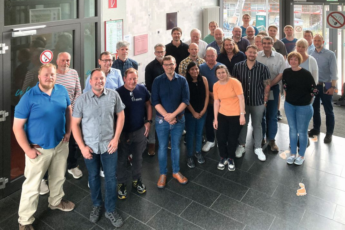
DGO District Group Thuringia - Dr. Jan Kinast, Group Leader Surface Technologies at the Fraunhofer Institute for Applied Optics and Precision Engineering IOF in Jena, was once again invited to speak. The Fraunhofer IOF in Jena develops and manufactures optical systems based on reflective metal optics for astronomy and space travel. Optical components are designed and simulated and realized using ultra-precise manufacturing techniques.
A highlight of the Fraunhofer IOF is the DLR Earth Sensing Imaging Spectrometer (DESIS). This enables high-resolution spectroscopic analyses of the earth from space, for example to make statements about vegetation density and water quality - such as suspended matter and organic pollution. In order to produce optical devices of the highest quality for use in space, high-phosphorus electroless nickel layers with an X-ray amorphous structure are deposited on metal optics, which later serve as a polishing layer. According to Dr. Kinast, the substrate and the NiP layer go through the following process chain: CNC milling of an aluminium part, diamond turning, NiP coating, diamond turning, MRF (magnetorheological finishing to correct the surface shape deviation) and CMP (chemical mechanical polishing) to minimize the roughness < 0.3 nm. The surface quality achieved is checked iteratively.
Three videos showed photos of the earth in high resolution and demonstrated how shape deviation, roughness of metal optics and diamond processing of electroless nickel coatings are related to this.
An additional challenge is the NiP coating of 3D-printed metal parts. After coating, diamond turning is carried out to achieve the required surface profile and also ends with CMP machining. Test mirrors with an internal honeycomb structure were presented. For special applications, chemically deposited coatings that minimize scattered light can be produced for optical systems. They exhibit low reflection on housing structures. After etching, these blackened electroless nickel layers show conical holes running perpendicular to the surface in the SEM image. Another field of optical coating production is NiP coatings on ceramic substrates. After grinding the ceramic substrate and the NiP coating, the layer was processed up to the final CMP stage. Dr. Kinast concluded his presentation with an overview of the IOF highlights in astronomy and space travel.
After the extensive discussion, DGO district group leader Mathias Fritz invited guests to a summer party with Thuringian delicacies from the grill and drinks.


