In its own development laboratory for printed electronics in Bronschofen, the Cicor Group carried out a technology evaluation in which various printing technologies were compared and assessed in terms of their suitability for the manufacture of products for the Group's customers and their target markets. These technologies included various inkjet options, screen printing and the aerosol jet printing process from Optomec.
In its own development laboratory for printed electronics in Bronschofen, the Cicor Group carried out a technology evaluation in which various printing technologies were compared and assessed in terms of their suitability for manufacturing products for the Group's customers and their target markets. These technologies included various inkjet options, screen printing and the aerosol jet printing process from Optomec.
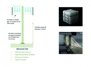
 Fig. 1: Schematic representation of the functional principle of an aerosol jet print head and examples of printed 3D silver conductive structuresThedevelopment laboratory for printed electronics is operated by the Group at its headquarters in Switzerland with the aim of jointly developing electronics applications together with customers. During the evaluation, aerosol jet technology proved to be the most suitable in this context.
The main advantages of this technology are its flexibility in terms of the choice of printable materials and shapes, the variety of available and printable inks and the print resolution, which is superior to that of the other processes evaluated. In addition, the operating principle significantly reduces the risk of clogged print heads and the associated maintenance costs.
Due to these advantages, the Cicor Group was chosen accordingly and a 5-axis printing system including the necessary infrastructure and measuring equipment was installed. This equipment has all the capabilities of this process.
Technology overview
As shown in Figure 1, the process uses an aerosol surrounded by a sheath gas to print the desired structure onto the surface of the workpiece. Several process steps are necessary to make this possible:
First, the ink is atomized in an atomizer, creating a mixture of nitrogen and ink droplets. This mixture is passed on to the print head with ink-specific parameters. Ink droplets that are too small or too large are sorted out, as they can have a negative impact on the print result.
In the actual print head, the ink jet is formed and coated with a stream of nitrogen gas. This technology makes it possible to focus the ink jet very precisely in order to achieve structure widths ranging from 10 µm to over 1 mm. Uniform printing results are achieved with variable distances to the substrate surface between 1-10 mm. If the topography or the structure heights are within this range, it is not necessary to move the print head or the workpiece in the z-axis.
Ink materials
The inks usually consist of a mixture of the material to be printed, polymer binders and two solvents, one of which has a high and one a low vapor pressure. The metal nanoparticles contained have an additional functional coating which ensures that the particles are kept in dispersion and that no sedimentation or segregation occurs.
A large selection of different inks is available:
- Metal nanoparticle inks (silver, gold, nickel, copper, platinum) with particle sizes of < 100nm
- Metal flake inks (silver) with flake sizes of max. 1 mm
- Non-metallic conductive inks (carbon, conductive polymers)
- Resistive inks (carbon, ruthenate)
- Dielectric inks (acrylates, polyimides)
- Piezo inks.
In order to make the right ink selection, it is necessary to precisely specify the requirements for the product, such as the desired conductivity or adhesion to the substrate. The most commonly used inks are currently based on silver nanoparticles. They offer the best balance between printability, material costs and coating properties, such as adhesion and conductivity/resistance.
Depending on the ink selection and the given viscosity, two different atomization processes are used. Inks with a low viscosity are usually atomized using ultrasound, while highly viscous inks are atomized using a pneumatic process.
Curing methods
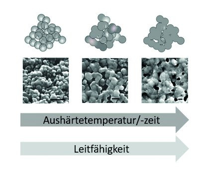
In order to achieve the final properties of a printed structure, the inks must be cured. In most cases, this curing - or sintering in the case of metal-based inks - is achieved by applying temperature. Typical curing temperatures for nanoparticle inks start at around 120 °C, depending on the metal used. During this curing process, organic components such as solvents are removed from the printed layer and the nanoparticles fuse together. This leads to the formation of a conductive path, whereby the conductivity generally increases with increasing curing temperature and time (see Fig. 2). The following processes are available for thermal curing:
- Thermal curing in a batch oven or continuous oven
- IR laser curing, the ink layer is heated locally with a laser after the printing process
- IPL (intense pulsed light), light pulses in the ms range selectively heat the ink to several 100 °C
Thermal curing in ovens is suitable for materials with a temperature resistance of > 120 °C. IR lasers and IPL are used for temperature-sensitive materials. With these methods, the temperature input is limited to the ink while the carrier material only heats up slightly. IPL is particularly suitable for light-colored or transparent substrates.
 Fig. 2: Schematic representation of the sintering process of a silver nanoparticle ink as a function of temperature and time with corresponding SEM images
For other inks - especially dielectric inks - a UV curing process is available as an alternative, depending on the type of ink.
Printable materials
The moderate curing temperatures of the inks used enable printing on a wide variety of different materials. The selection of suitable materials depends on the specified coating properties. The temperature and solvent resistance of the substrates used provide crucial information that is of great importance for the selection of suitable inks.
The following materials were successfully tested for their printability:
- Plastics: PEEK, LCP, ABS, polycarbonate, POM, PBT
- silicone
- Polyimide and LCP films
- glass
- Al2O3 and AlN ceramics
- Metals, steel
- Parylene
- paper
The substrates to be printed on require suitable pre-treatment to ensure sufficient wetting and adhesion. Metallic workpieces must be provided with an insulating layer to avoid short circuits, porous materials must be prepared with a primer layer to be able to print uniform structures.
Reliability of the printed structures
One of the decisive factors for the usability of printed structures is their reliability under harsh or changing environmental conditions. The defining factors for this are the properties of the materials to be printed and the inks used, as well as their compatibility. Increased resistance and possible degradation of ink adhesion were used as test and failure criteria.
As a reference, the resistance values of the printed layers after the curing process were determined using a 4-point measurement. Cross-cut tests with subsequent adhesive tape peel tests were used to assess the adhesive strength.
The following test methods were selected to evaluate reliability:
- Temperature storage for 280 hours at 150 °C
- Temperature cycling test: -40 / 125 °C, 500 cycles
- Climate test at 85 °C / 85 %RH for 168 hours
Following these tests, the resistance measurements were carried out again on the same structures and the percentage change was determined. In addition, the change in adhesive strength was also evaluated by carrying out cross-cut and adhesive tape tests again.
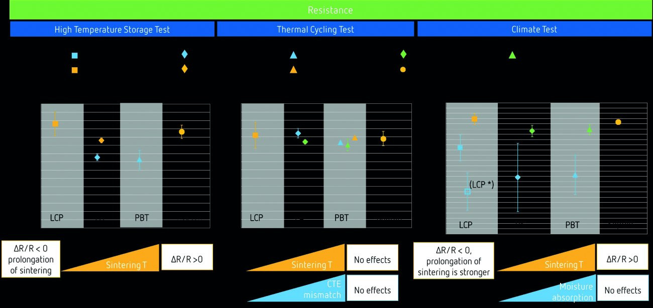
 Fig. 3: Resistance change in the 3 test methods used show no resistance increases in a range of more than 5 %
As can be seen in Figure 3, a maximum resistance increase of 4 % occurs during the tests. For materials with low temperature resistance, there is a reduction in resistance, especially during the climate test. This can be explained by the continuing sintering process, which leads to further fusion of the nanoparticles.
No significant degradation was detected in the adhesion tests; the adhesion is still within the specified range after these tests.
Component bonding to printed silver structures
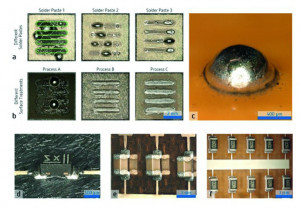
 Fig. 4: Images a+b show the wetting of different solder pastes in combination with the pre-treatment of the printed layers. Figure c shows the example of a solder ball on which shear tests were subsequently carried out. Figures d+e+f show various passive components soldered onto different printed substratesThereare several ways of attaching electronic components to structures printed using the aerosol jet process. In addition to mechanical technologies such as connectors or spring contacts, there is also the option of soldering components.
Due to the structure of the silver layer, processes using standard solders are not suitable. This is due to the fact that the conductive structure consists of a mixture of silver particles and polymer binders. The silver particles alloy in standard solders due to the high temperatures, which can lead to an uncontrolled reduction in the layer thickness. In addition, the thermal stress starts the decomposition of the polymer binders present in the layer.
Furthermore, pre-treatment of the printed soldering surfaces is essential in order to remove these binders from the surface and make pure silver accessible for the soldering process. The soldering process is carried out with low-temperature solders, which is the only way to ensure that a sufficiently thick functional silver layer remains after the placement process.
The ball shear tests carried out to evaluate the quality of the solder joints show no cracks on the solder interface if the correct pre-treatment and suitable soldering parameters are selected. Typically, cracks occur in the solder ball or at the interface between the printed silver ink and the base material. The shear test values can be significantly increased again by optimizing the design of the printed structures.
Summary
The Aerosol Jet Printing technology used by Cicor offers significant advantages over comparable methods in terms of flexibility, resolution and ease of maintenance. The use of this technology opens up possibilities that previously could not be realized, or only at great expense. If emphasis is placed on the selection of suitable material combinations in the early stages of a project and design rules are followed, this technology is suitable for manufacturing highly reliable and cost-efficient products. The 3D capability and the ability to print very fine structures means that a very high level of functional integration can be achieved. Several methods are available to connect the printed circuits to electronic systems and components can be soldered on. As this is a relatively new technology, close cooperation between development partners is crucial, especially at the start of a project. The Cicor development team will be happy to support you in implementing your ideas.


