
Already today, about 40 % of the energy converted worldwide by technical systems is provided in the form of electric power. This share is expected to rise to around 60 % in 2040. These huge amounts of energy must not only be generated in a way that conserves resources and protects the environment, but must also be distributed and used efficiently.
Already today, around 40 % of the energy converted by technical systems worldwide is provided in the form of electricity. This proportion is expected to rise to around 60 % by 2040. These huge amounts of energy not only have to be generated in a way that conserves resources and the environment, but also distributed and used efficiently.
The power electronics required for this is an 'emerging field' of electrical engineering that makes it possible to provide electrical energy optimally adapted to a wide range of applications. These applications include the integration of renewable energy sources into the electrical supply network, drive technology for electromobility, the power supply of data centers or the high-frequency network of mobile telephony. When considering the power electronics components used for these applications over their service life, it becomes clear that increasing their energy efficiency not only opens up a market advantage, but can also significantly reduce the associated carbon dioxide equivalents. The current development and evaluation of particularly energy-efficient gallium nitride-based (GaN) power electronics components and circuits clearly shows the high potential for energy savings offered by the further optimization of semiconductor materials and microelectronic components and the way in which they can be used to create more sustainable, application-relevant components.
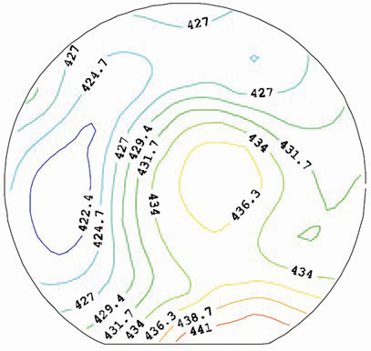

Distribution of sheet resistances (given in Ω/□) of Ga0.75Al0.25N/GaN- (left) and Sc0.2Al0.8N/GaN-based heterostructures with a diameter of 100 mm determined using eddy current measurements
Compared to comparable, conventional silicon components, GaN-based high electron mobility transistors (HEMT) open up the opportunity for particularly energy-efficient and yet marketable power electronic circuits. HEMTs are processed industrially from Ga0.75Al0.25N/GaN heterostructures, which have polarization-induced two-dimensional electron gases at their interface with a very high charge carrier surface density of around 8 x 10¹²/cm2 and enable channel resistances of only 400 Ω/□ due to the high electron mobility. The low channel resistances and gate capacitances in combination with the high breakdown field strength of GaN-based HEMTs enable voltage converters with switching edges of more than 200 V/ns. Current research work shows that new switching topologies and concepts can be implemented using the switching edges achieved, which significantly reduce the size and costs of voltage converters. In addition to saving on components, these topologies enable the realization of power electronic components with an energy efficiency of >98 % at an output power of more than 1000 W [1]. National research groups have also succeeded in demonstrating high-frequency power amplifiers with output powers of almost 1000 W at an operating frequency of 1000 MHz and a power efficiency of 60 % for use in mobile phone base stations. These performance data describe the state of the art of GaN-based high-frequency power amplifiers, without the theoretically predicted potential of GaN technology having been fully exploited to date.
Despite the outstanding performance of GaAlN/GaN HEMT already achieved, there is a great need for transistors with even higher output powers and high energy efficiency. One option to further increase the output power is voltage scaling, i.e. the optimization of electric field distributions in GaAlN/GaN HEMT to operate at higher drain voltages. Leoni et al [2] reported operating voltages of up to 200 V, enabling HEMT output powers per gate width of up to 51 W/mm. However, voltage scaling reduces the bandwidth of GaAlN/GaN-based power amplifiers and is therefore limited to microwave frequencies. To overcome this limitation, the transistor current density must be increased proportionally to the scaling of the operating voltage. Therefore, the current challenge is to develop HEMTs that allow both current density and operating voltage to be increased.
To this end, the Ga0.75Al0.25N barrier of the HEMT is currently being replaced by a thin scandium aluminum nitride (Sc0.2Al0.8N) layer. The deposition of high-quality, single-crystalline ScAlN layers on GaN has only become possible in recent years thanks to the epitaxy processes of molecular beam epitaxy (MBE) and metal organic vapor deposition (MOCVD) [3, 4]. These processes have resulted in the availability of Sc0.2Al0.8N/GaN heterostructures, which enable the processing of HEMT with electron surface densities of up to 30 x 1012/cm2 and channel resistances of less than 200 Ω/□ [5]. Another advantage for the performance of the novel HEMT is that the Sc0.2Al0.8N barrier (≈ 5.3 eV) has a larger bandgap compared to the Ga0.75Al0.25N layer (≈ 3.9 eV) and can be fabricated unbonded. Both the larger bandgap and the higher possible barrier thickness support an upscaling of the operating voltage of ScAlN/GaN- compared to GaAlN/GaN-HEMT.
Raytheon Technologies and the Air Force Research Lab in the USA have already demonstrated ScAlN/GaN-HEMT on SiC substrates with maximum current densities of 3 A/mm - values that are far above what can be achieved with today's GaAlN/GaN-HEMT comparable designs [6, 7]. These transistors exhibit slopes of up to 0.5 S/mm, low leakage currents in the blocking state (<1 mA/mm) and breakdown voltages of over 60 V. The components have a transit frequency (ft), a maximum oscillation frequency (fmax) and a maximum gain (Gmax) of > 50 GHz, > 140 GHz and 13 dB.
The combination of the measured power and high-frequency characteristics of the ScAlN/GaN HEMT indicates its potential for particularly energy-efficient power amplifiers with applications in mobile communications. The low channel resistance and the high operating voltage of the transistors achieved with short gate lengths also promise a significant increase in the output power and efficiency of GaN-based voltage converters. The estimated savings in the operation of power electronic systems motivate the development of ScAlN/GaN-based power electronic components through to their production, both from an economic and an environmental point of view.
Prof. Dr. Oliver Ambacher will be honored for this research work by the German Vacuum Society DVG e. V. with the Rudolf Jaeckel Prize 2021 at V2021 on October 12, 2021. The award is in recognition of his outstanding achievements in the fields of science and technology supported by the DVG, in particular for his pioneering contributions to the progress of power electronic systems through the development of devices made of novel semiconductor structures based on materials with a large band gap. The award ceremony will take place at the symposium V2021 Vacuum & Plasma (12-14 October 2021, ICC Dresden) organized by the European Research Association for Thin Films (EFDS). In addition to the prizewinner's lecture on 12 October 2021, there will be a wide range of technical presentations on the energy transition through thin films, vacuum technology, hydrogen technology, digitalization and surface technology in practice. Numerous exhibitors will present their offerings in vacuum technology, surface technology and electrical engineering.
About the person
 Prof. Dr. Oliver Ambacher has once again headed the Fraunhofer Institute for Applied Solid State Physics IAF since January 1, 2018. From 2007 to the end of 2016, the physicist was already at the helm of the Freiburg-based Fraunhofer Institute and has now been appointed as Institute Director for the second time.
References
[1] S. Mönch, et al, Phys. Stat. Sol. A 218, 2000404 (2021)
[2] R. Leoni, et al, IEEE Compound Semicon-ductor Integrated Circuit Symposium (2017)
[3] M. T. Hardy, et al, IEEE Trans. Semicond. Manuf. 30, 475 (2017)
[4] S. Leone, et al, Phys. Stat. Sol. RRL 14, 1900535 (2019)
[5] O. Ambacher, et al, J. Appl. Phys. 129, 204501 (2021)
[6] T. E. Kazior, et al, IEEE MTT-S Int. Microw. Symp. Dig. 1136 (2019)
[7] A. J. Green et al, IEEE Elec. Dev. Lett. 41, 1181 (2020)
