In the development and manufacture of many electronic devices, new and enhanced functionalities must be realized in the smallest possible space. Advanced packaging - the complex assembly and interconnection of semiconductor components - has emerged as an essential technology for the integration of photonics, optics and electronics.
") The researchers are developing a thin and flexible polymer substrate including very thin, embedded electronic components for biocompatible patches that have to be adapted directly to the skin (this and cover picture)In the development and manufacture of many electronic devices, new and enhanced functionalities have to be realized in the smallest possible space. Advanced packaging - the complex assembly and connection technology of semiconductor components - has therefore emerged as an essential technology for the integration of photonics, optics and electronics.
The researchers are developing a thin and flexible polymer substrate including very thin, embedded electronic components for biocompatible patches that have to be adapted directly to the skin (this and cover picture)In the development and manufacture of many electronic devices, new and enhanced functionalities have to be realized in the smallest possible space. Advanced packaging - the complex assembly and connection technology of semiconductor components - has therefore emerged as an essential technology for the integration of photonics, optics and electronics.
In the current EU project Applause, the participants are focusing on the development of new tools, methods and processes for the mass production of electronic and optical components in large quantities. Fraunhofer IZM is involved in three of six use cases.
A consortium consisting of 31 European key players from the fields of electronics packaging, optics and photonics, leading equipment suppliers and test experts is driving the project 'Advanced packaging for photonics, optics and electronics for low cost manufacturing in Europe' (Applause for short). The project promotes the European semiconductor value chain by developing new tools, methods and processes for high-volume manufacturing. In addition to 12 large companies, 11 small and medium-sized enterprises and 7 research and technology organizations, the Fraunhofer Institute for Reliability and Microintegration IZM is also involved. In addition to various other exciting projects, the researchers in Berlin are involved in three industrial application fields and are working on the creation of
- a low-cost infrared camera for automotive and surveillance applications
- a high-speed datacom transceiver
- a flexible patch for cardiac monitoring
Safer in traffic thanks to thermal infrared sensor
As part of the first use case, the consortium partners are developing a camera for generating thermal images with increased video rates and VGA resolution for automotive and security applications using a low-cost microbolometer. A microbolometer is a thermal sensor for detecting electromagnetic radiation, for example in situations where visible light is no longer sufficient. The microbolometer consists of a multi-layered yet wafer-thin membrane with an infrared-sensitive absorber layer. The membrane is suspended in a vacuum with two tiny electrodes and is therefore thermally insulated. The incident infrared radiation heats the thermally insulated membrane through resonance, which leads to a change in the electrical resistance of the sensor layer. This changes the measurement signal, which is recorded by a readout circuit. As the individual membranes are arranged in a flat grid on the readout circuit, this results in a pixel matrix. The result is a camera sensor for recording infrared images.
The aim of the project is to produce a low-cost, high-performance thermal infrared sensor. As a vacuum environment is required for the microbolometer to function properly, the researchers at Fraunhofer IZM are using a special packaging process for robust hermetic encapsulation. They cover the fine, densely packed microbolometer structures at wafer level with a cap wafer that has windows for infrared transmission. This not only protects the highly sensitive sensor elements for further integration into the final camera sensor, but also hermetically seals them under vacuum to ensure their complete functionality.
Faster data communication with high-speed transceivers
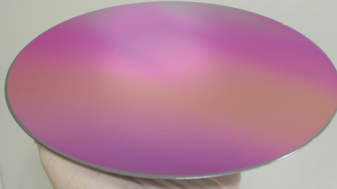
 Researchers use special wafer packaging processes to hermetically seal the thermal sensor in an infrared camera: A 200 mm diameter cap wafer encloses the sensors under vacuum, creating an external anti-reflective coatingThesecond application involves communicating and analyzing data. Here, ever higher speeds are a constant driver for further developments. Therefore, a cost-effective 400 Gb/s high-speed optical transceiver for data communication is one of the next milestones in this area. To this end, Fraunhofer IZM is developing an ambitious optical silicon bank for the transmission unit (transceiver). The special feature here is the planned passive alignment of the components, which is intended to shorten and simplify sub-micrometric, high-precision assembly for large quantities. Assembly costs could thus be significantly reduced compared to the current state of the art. The combination of silicon microstructuring and gold-based metallization for the high-frequency signal rewiring and the flipchip solder contacts produces a 3D substrate for optical elements (lens, isolator, fibre) including mechanical stoppers. This allows the laser-emitting device (EML) to be mounted with a precision of less than 1 μm. The approach benefits from the close collaboration with Almae Technologies in the project. Another exploratory approach for the integration of optical elements is a 3D-printed substrate, which is being tested in parallel.
Biocompatible patches diagnose directly on the skin
The digital age is also driving the development of monitoring technologies through wearables such as fitness trackers and smartwatches. But cardiologists still need alternative technologies for their diagnostic and monitoring tasks. This is where flexible electronics come into play. Such monitoring devices require close contact with the skin. Electronic components must be integrated into flexible and even stretchable layers that can adapt ideally to the skin. Fraunhofer IZM's third contribution to Applause deals with the integration of thin components in a thin and flexible polymer substrate including a rewiring layer. The technologies developed for stretchable electronics based on thermoplastic polyurethane will make it possible to integrate electrodes and electronics into a compact, flexible and biocompatible patch.
The applications outlined clearly illustrate the great potential of advanced packaging technologies for the future. In the overall project, the expected impact is an increase in sales of over €300 million by 2025. The new technologies have the potential to increase market share and provide industry partners with additional access to new market segments. The three-year Applause project is co-funded by the EU under Horizon 2020 and national funding organizations and industry as part of the Electronics Components and Systems for European Leadership Joint Undertaking (ECSEL JU) with €34 million.
