In collaboration with project partners, scientists at the Fraunhofer Institute for Laser Technology ILT have succeeded in developing a new type of industrial manufacturing process. It now enables cost-effective FR4 PCB substrates to be used in power electronics, for example in electric motors.
Scientists at the Fraunhofer Institute for Laser Technology ILT, in collaboration with project partners, have succeeded in developing a novel industrial manufacturing process. It now enables low-cost FR4 circuit board substrates to be used in power electronics, for example in electric motors.
Compared to the use of conventional ceramic circuit boards, the so-called hybrid circuit boards are not only much more versatile, but also up to 20 times cheaper. This could close a gap in the market in the medium term and thus make an important contribution to the mobility of the future.
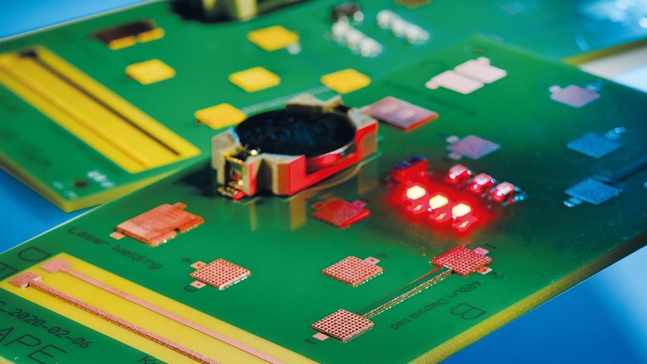
July 29, 2021 was Earth Overshoot Day - the day on which we humans used up the natural resources of our planet. This means that by the end of the year, we will be living and consuming at the expense of our planet - a situation that research has long been pointing out. With the climate transition project, politicians and industry are increasingly addressing the need to end our society's extreme dependence on fossil resources as quickly as possible.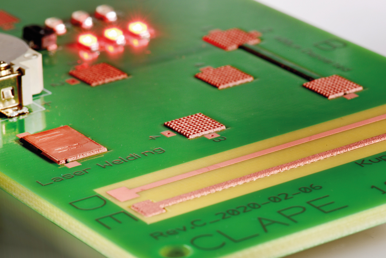 Fig. 2: Demonstrator for the combination of cold gas spraying and laser-based joining
The term "energy transition" has been circulating in scientific discourse since the 1980s. The starting point was the environmental and anti-nuclear movement of the 1970s. However, it has only been widely implemented since 2015, when 196 member states of the United Nations signed the Paris Climate Agreement. This is having an increasing impact on the way we generate and use energy - and the technologies we use to do so. In particular, the mobility transition as an important component of the energy transition is the focus of interest. One of the key objectives is to switch from combustion engines to electromobility. This will significantly increase the demand for technologies to generate electrical energy, which has already risen sharply in the recent past.
In the BMWi-funded project CLAPE ('Innovative Cold Spray Deposition and Laser Joining for PCB Based Power Eletctronics'), experts from Fraunhofer ILT, ILFA GmbH and the French SME Ouest Coating have successfully tackled this challenge over the past three years. They developed a new process for manufacturing printed circuit boards such as those used in electric vehicles. It saves weight and space and could also reduce costs in the future - as well as leading to a significant reduction inCO2 emissions.
One component, multiple functions
"Imagine a copper block with the same surface area but different thicknesses in cross-section," says project manager Woo-Sik Chung from the Micro Joining Group at Fraunhofer ILT, breaking down the principle of the newly developed manufacturing process to its essence. "The thicker the block, the greater the current transfer. We reinforce the circuit board where the most current is needed. Where only a small amount of current needs to flow through, we save material."
This was achieved by the experts involved in the CLAPE project developing a new process with which specific areas of a printed circuit board were thickened so that a welded connection could be made. This was previously not possible using standardized manufacturing processes such as classic laser welding. This is because conventional PCBs are usually made of ceramic. Laser beam welding, on the other hand, releases so much energy that the material would be significantly damaged. To prevent this from happening, a metallization with a higher heat capacity is required, i.e. a larger amount of heat that the component can absorb at a certain temperature change.
"Until now, the rule was: you use a PCB with thin metallization or thicker. Either-or. Depending on the application," explains Chung. "A current transformer for charging batteries in electric cars, for example, requires a lot of current within a short period of time to transmit power. In contrast, only a few milliamperes are needed to transmit a current signal to an LED light. Our new production process makes it possible to realize both on just one PCB at the same time: Signal and power transmission."
The advantage of the newly developed process is that it makes it possible to use multilayer PCBs based on conventional, cost-effective FR4 substrates, even with energy-intensive welding processes. These would be thermally damaged in conventional welding processes. In addition, thanks to their specific design for signal and power transmission, the hybrid PCBs produced require significantly less power than conventionally manufactured PCBs. This not only saves space, but also large amounts of energy overall, as this can be distributed much more efficiently (see Fig. 2).
Combination of proven processes
The experimental set-up comprised three phases: lamination, layering of the material, i.e. thickening, and the welding process. Two proven processes were combined in a new way: cold gas spraying and laser micro welding.
In the first step, a copper layer around 18 μm thick was laminated onto the FR4 substrate. This served as a bonding layer between the copper powder applied in the second step by cold gas spraying and the FR4 substrate. By applying a thin layer of copper powder, the experts thickened it only in those places where it was functionally necessary and desired. This created a copper layer whose material properties corresponded approximately to the theoretical material density and thermal conductivity. This minimized the likelihood of negative effects occurring during laser beam microwelding and due to the local power modulation of the laser beam. As a result, differently reinforced conductor tracks could be welded to the printed circuit board using laser beam microwelding - without being significantly damaged by excessive thermal stress.
Compared to other thermal spraying processes, the cold gas spraying process is particularly suitable for metallizing temperature-sensitive materials and substrates due to its relatively low energy consumption. Even if the copper base metallization laminated on the substrate is only wafer-thin at 18 μm, as in the application case, the substrate was hardly damaged. The bandwidth with which the cold gas spraying process could be used is correspondingly large. The applied copper layer could be reinforced up to 600 μm.
The biggest challenge here was to take into account the rough surface finish and the uneven heat distribution when applying the copper layer. The energy of the laser beam had to be regulated in such a way that the applied copper layer melts homogeneously despite the rough surface and bridges the gap between the two joining partners.
The background: When steam escapes during welding, it exerts pressure on the molten metal and partially displaces it. The workpiece melts even further. A deep, narrow, steam-filled hole forms, a steam capillary. This had to be prevented as far as possible. The surface quality and the energy of the laser have a decisive influence on this. The coarser the copper powder, the rougher the layer applied by cold gas spraying. The higher the energy impact, the deeper the vapor capillaries, which result in deeper penetration of the melt into the material (see Figs. 3 and 4). This relationship needs to be investigated further in the follow-up projects. The aim is to optimize the processes until they are ready for the market.
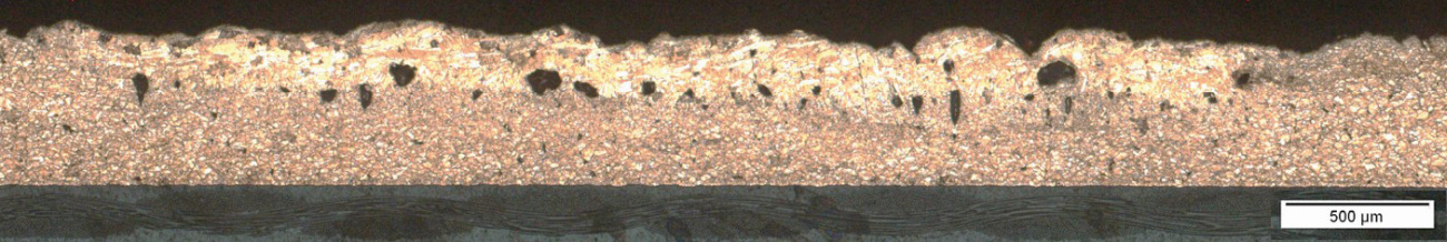 Fig. 3: Longitudinal section of blind weld on sprayed copper layer
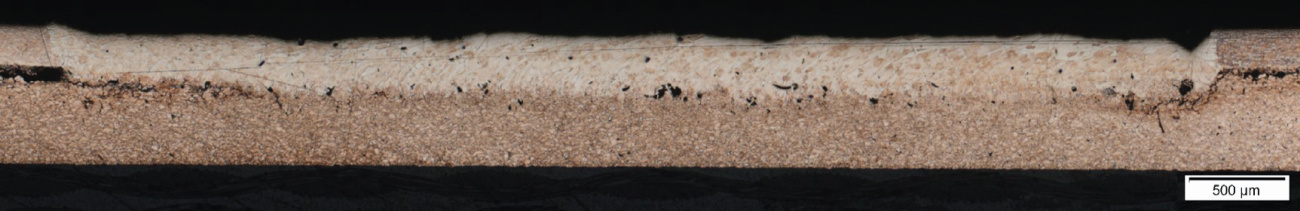 Fig. 4: Longitudinal section of welded sample with low surface roughness
Exploiting further potential
"If the process becomes established in practice, our hybrid printed circuit boards could combine several functions within one component in the future," says Woo-Sik Chung. "We could significantly reduce the installation space for the power electronics and the overall weight of electric cars, which would result in both a longer range and lowerCO2 emissions in the long term." This is also an extremely important finding in view of the fact that the resources required to manufacture chips for power electronics are scarce.
The fact that the higher efficiency is also accompanied by greater cost-effectiveness makes the new development from Fraunhofer ILT particularly interesting for industry. Especially when you consider Germany's recently revised climate targets, which aim to cutCO2 emissions by 65% by 2030 and make the country climate-neutral by 2045. Instead of a few central electricity suppliers, there should then be a decentralized network of many energy suppliers. Solar cells, for example, private biogas and wind power plants. Another central component of the strategy is e-mobility. In the future, e-car batteries could store or supply energy. Depending on demand.
The most important drivers of innovation in this area include the electronics and chemical industries in particular, with their decades of experience. This is illustrated by a study by the Vienna Future Institute. According to the study, traditional car manufacturers have more than 60% of the expertise in combustion engines, but only 15% in electric motors. Knowledge of conventional engines and transmissions therefore only seems to play a subordinate role for e-mobility. New technologies are therefore in demand in the mobility sector and beyond, such as the production process for hybrid circuit boards in power electronics developed in CLAPE.
"We only recently completed the project," says Chung. "The technology is not yet ready for the market and some adjustments are still needed before it can be used in practice. However, we have already been able to show that there are promising technological alternatives to the status quo." The next research goal is now to optimize the energy input and further reduce costs. "We still have room for improvement here. However, this also shows us the great potential of the technology as soon as it can be used profitably."
The CLAPE project partners:
- ILFA GmbH, Hanover (printed circuit boards, demonstrator construction)
- Ouest Coating, Saint Nazaire / France (cold gas spraying process)
- Fraunhofer Institute for Laser Technology ILT, Aachen (laser-based joining technology, project management)
The CLAPE project was funded by the German Federal Ministry for Economic Affairs and Energy (BMWI). The project sponsor was Aif Arbeitsgemeinschaft industrieller Forschungsvereinigungen 'Otto von Guericke' e. V.
Further information:
Contact: Woo-Sik Chung M. Sc. Fraunhofer ILT, Micro Joining Group Phone +49 241 89 06 - 322
W.-S. Chung, G. Jo, A. Olowinsky: "Investigation of the laser-based joining technique for PCBs with locally thickened layers using a cold gas spraying process", Proc. SPIE 11674 (2021); doi:10.1117/12.2585101
Images: Fraunhofer ILT, Aachen
