Silicon and glass have similar thermal expansion coefficients. In the case of substrate materials, temperature changes during operation and production lead to expansion and shrinkage, which result in significantly less stress for glass core substrates. Their development and market success are being observed with corresponding enthusiasm.
Silicon and glass have similar coefficients of thermal expansion. With substrate materials, temperature changes during operation and production lead to expansion and shrinkage, which results in significantly less stress with glass-core substrates. Their development and market success are being watched with corresponding enthusiasm.
Currently, organic substrates are predominantly used as carrier materials for semiconductor dies, having replaced ceramic substrates in most application areas decades ago. However, they are now increasingly reaching their limits in selected future segments. Prominent examples of this are high-end processors for data centers with several semiconductor chips on one substrate and the new AI computing bolides with their extreme hunger for performance and data throughput. Not only industry giants such as Intel and Samsung are involved in the development of glass core substrate technology, but also, for example, the start-up Absolics, a subsidiary of the Korean company SKC. The core tasks of the substrates are the mechanical stabilization of the semiconductor chips mounted on them, the necessary wiring between the chips and the electrical connections to the outside world (motherboard). Conductor tracks and connection holes (vias) are the main structural elements.
Advantages of glass core substrates
In contrast to organic substrates, silicon and glass have very similar thermal expansion coefficients. Temperature changes during operation and production lead to expansion and shrinkage, which result in significantly less stress for the better adapted glass core substrates. As the surfaces of the glass core substrates are significantly smoother than those of the organic substrates, much finer structures can be realized. This applies to both conductor paths and vias. According to Intel, the new substrates can accommodate around 50% more semiconductor chips than organic substrates. According to Intel, the maximum package size for the new glass core substrates is 240 mm x 240 mm compared to around 120 mm x 120 mm for organic substrates, quadrupling the maximum area, which will open up new possibilities, particularly for high-end processors for data centers (HPC) and AI chips. Narrow copper traces, closely spaced glass vias and extremely low dielectric losses of the glass material allow higher signal frequencies/data rates.
 Examples of processes for laser-assisted etching of glass cores
The challenges
Rahul Manepalli, head of the development department for substrate packaging technology at Intel, also addresses the stumbling blocks of glass as a substrate material: "It comes with very challenging integration and interface issues that we need to solve."[1] These include fragility, problematic adhesion to metal (wires) and the difficulty of creating a uniform via for consistent electrical power (P). Glass also differs fundamentally from silicon due to its transparency and different reflection behavior, so that measurement and inspection methods used for non-transparent and semi-transparent materials produce no or only partially reliable results. The translucency of glass can lead to signal distortion or loss during optical measurements. Keith Best, Director Product Marketing at the American semiconductor manufacturer Onto Innovation, summarized the challenges in a blog post for the website 'Semiconductor Engineering' in September 2023: "Glass is fragile, especially in the large shapes used today (510 mm x 515 mm and 600 mm x 600 mm). In addition, the glass substrate is very thin, in some cases < 100 μm." To minimize the risk of breakage, sophisticated processing and handling equipment is required. As a compromise, Keith Best describes a hybrid solution in which the large RDL structures are structured using the CCL base process and fine RDLs are structured on a glass substrate, which is attached to the CCL using tiny Cu bumps (microbumps). [2]
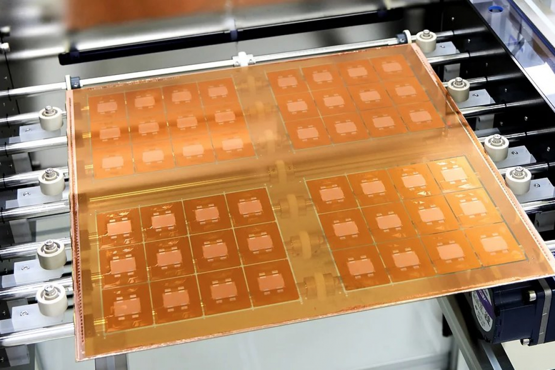
") Glass core substrate from Intel, presented in July 2023 in Chandler, Arizona (USA)
Glass core substrate from Intel, presented in July 2023 in Chandler, Arizona (USA)
Glass core substrates on the upswing
According to market analyses by the Yole Group, a market research company based in Lyon (France), the market for advanced IC substrates is expected to reach a value of USD 16.6 billion in 2024 and a compound annual growth rate (CAGR) of 9% between 2024 and 2029.[3] New players have entered the market for glass core substrates. Yole includes Absolics as well as the established companies Intel and Samsung. According to Yole, the forecast growth will be driven by the increasing demand for flip-chip ball grid array substrates and advanced 2.5D/3D packages. They are used in high-performance computers and data centers, 5G, CPUs and XPUs for AI personal computers and in the automotive sector. Upcoming market players will primarily focus on companies in the AI industry. The production of advanced IC substrates is mainly concentrated in Taiwan, Japan and South Korea, according to Bilal Hachemi, analyst at Yole. China has also made significant progress since 2021 after investments and will gain market share in the future, especially for FCBGA substrates. The supply chain for substrates in the USA, on the other hand, is only developing slowly. However, this has changed thanks to a government subsidy program for substrate production in the USA. However, Yole assumes that the production of advanced IC substrates will continue to be concentrated in Asia. For example, Zhen Ding, headquartered in Taiwan, is investing over $1 billion by 2027 to become a global supplier of high-end substrates. Zhen Ding topped the list of the world's largest PCB manufacturers in the 2023 NTI 100 report[4].
www.intel.de, www.absolicsinc.com, www.ontoinnovation.com, www.yolegroup.com
References
[1] https://semiengineering.com/the-race-to-glass-substrates/ (Retrieved: 27.10.2024).
[2] https://ontoinnovation.com/writable/files/Intelligent-Innovation-The-Glass-Substrate-Formatted.pdf (accessed: 27.10.2024).
[3]https://www.yolegroup.com/press-release/advanced-ic-substrate-industry-exciting-developments-on-the-horizon/(Retrieved: October 21, 2024).
[4] PLUS 10/2024, p. 1220ff.
