The following article provides an overview of joining processes used in electronics production from the sintering technology sector. They are used in lighting (LED and others), healthcare, industrial electronics, automotive electronics and power electronics. Part 1 of the article explains the sintering process itself and some application examples. Part 2 takes a closer look at technology variants.
The following article provides an overview of joining processes from the technology area of sintering used in electronics production. They are used in lighting (LEDs and others), healthcare, industrial electronics, automotive electronics and power electronics. Part 1 of the article explains the sintering process itself and some application examples. Part 2 goes into more detail about technology variants.
Introduction
Sintering technology is a joining process especially for the fields of ligthing, healthcare, industry, automotive and power electronics [45]. By using the miniaturization of the joining materials, e.g. silver and copper and/or material mixtures or metallized ceramic and metallic coated particles, the remelting characteristics are shifted to higher temperatures. This makes sintered compounds suitable for high-temperature applications in the above application areas. The following paper attempts to provide an overview of technology variants and material variants for sintering technology. The evaluation of international meetings and conferences is the focus here - they are listed below:
- ECTC 2017 67th Electronic Components and Technology Conference
- ECTC 2018 68th Electronic Components and Technology Conference
- ECTC 2019 69th Electronic Components and Technology Conference
- EMPC 2017, European Microelectronics and Packaging Conference
- EMPC 2019 European Microelectronics and Packaging Conference
- ECPE Workshop 2019, ECPE Workshop Advanced Power Packaging - Power Modules 2.0
- CIPS 2018 10th International Conference on Integrated Power Electronics Systems
- ESIME 2018 19th Annual International Conference on Thermal, Mechanical and Multi-Physics Simulation and Experiments in Microelectronics and Microsystems
- ESIME 2019 20th Annual International Conference on Thermal, Mechanical and Multi-Physics Simulation and Experiments in Microelectronics and Microsystems
- IMAPS 2019 European Microelectronics and Packaging Conference
- PCIM 2017 International Trade Fair and Conference for Power Electronics, Intelligent Drive Technology, Renewable Energy and Energy Management
- PCIM 2019 International Trade Fair and Conference for Power Electronics, Intelligent Motion, Renewable Energy and Energy Management
- EBL 2018 Electronic components and printed circuit boards
- ESTC 2018 7th Electronic System-Integration Technology Conference.
The following recognizable trends for high-temperature connections are examined and evaluated in more detail in this article.
Sintering technology
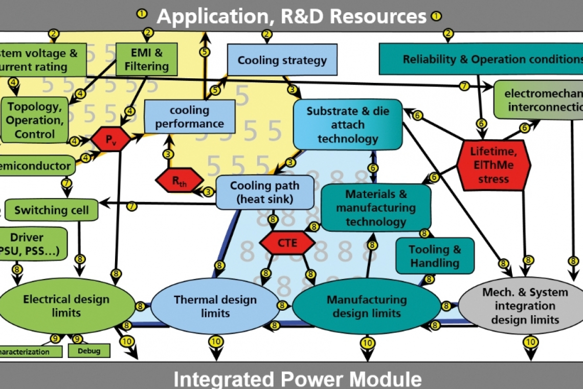
Figure 1 shows factors influencing the sintering process. A very good overview of technology and process variables was published in [1]. For integrated power modules, the design limits with regard to electrical, thermal, manufacturing, mechanical and system integration are discussed here. Based on this, the materials and assembly technologies that ultimately result in or influence the lifetime are presented. Mission profile and operating conditions are the starting points for calculable technology variants. Examples of the power modules are shown in Figure 1.1.
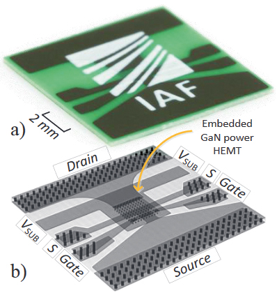
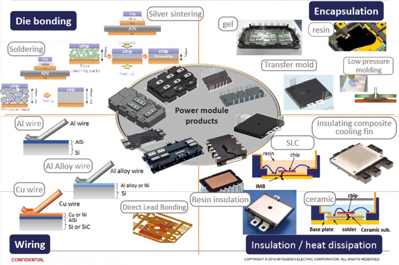 Fig. 1.1: Power modules [45]
The variants of the technology application for high-temperature connections are presented in [2] and are visualized in Figure 2. In addition to the established soldering technology, diffusion soldering, press contacts and sintering technology are described. In the context of sintering technology, the focus is on low temperature sintering technology under pressure and without pressure, whereby low temperature sintering technology is to be defined (see Fig. 3).
 Fig. 2: Chip interconnection techniques for power modules [2]
The sintering technology application is developed and used for Ag sintering (SiC, GaN) as well as Cu sintering. The special process engineering features will have to be analyzed in particular through the use of inert or shielding gas applications. In order to bond SiC/GaN securely to the substrate, the die-bonding materials must have higher temperatures in the environment and excellent thermal and conductive properties in order to meet the reliability requirements.
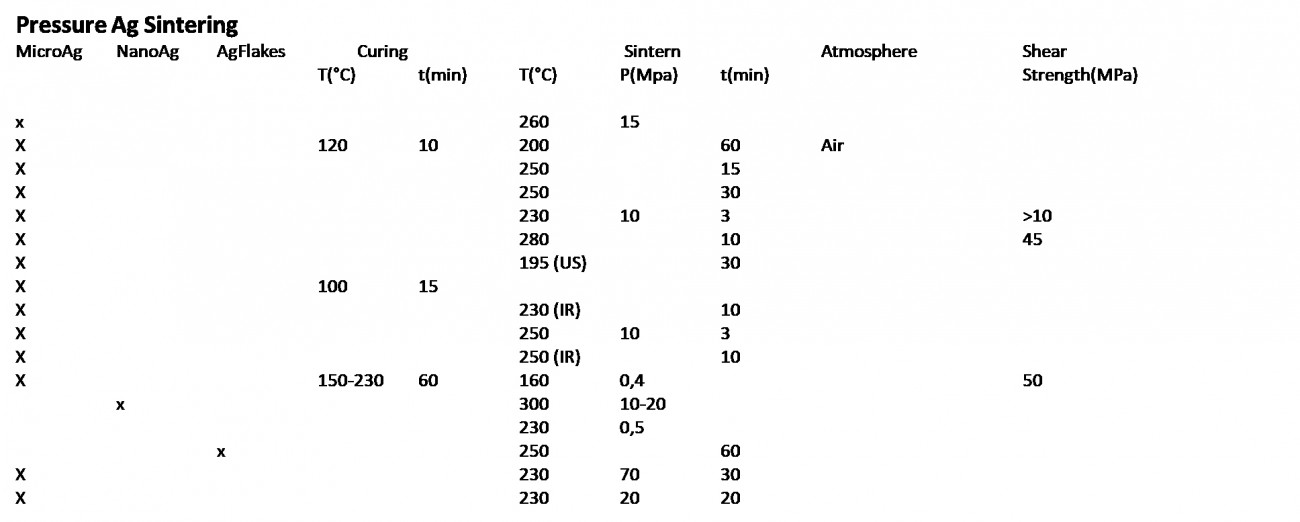
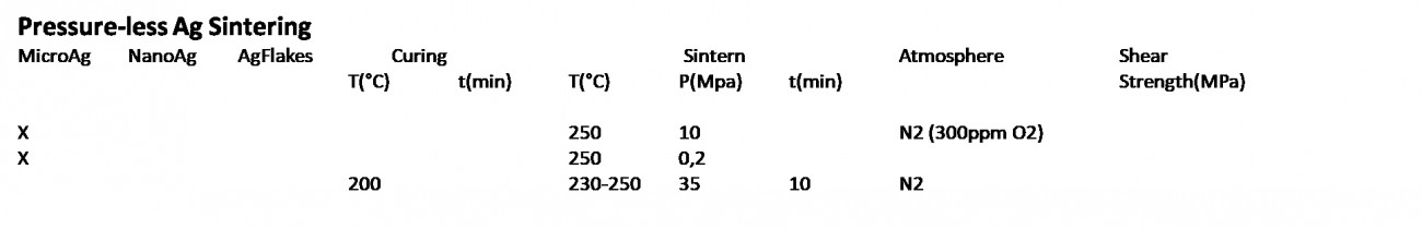
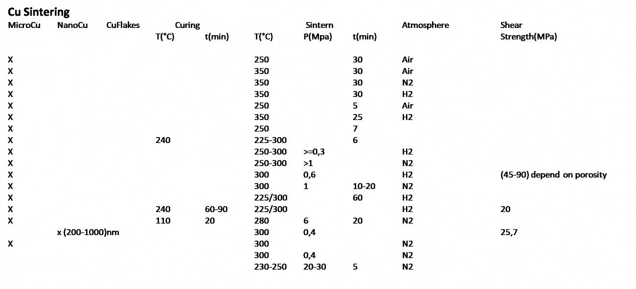 Fig. 3: Ag and Cu sintering process parameters [3-43, 64, 65,79]
The following diagram provides an overview of the technology and process variables. The parameters preheating, temperature, pressure and sintering time, sintering atmosphere and shear strength (where specified) are shown here. It is also noticeable that the nano-powder is no longer given any importance. The variable sintering pressure must be standardized in order to be able to compare the different designs. SiC modules can guarantee e.g. 1000 cycles between -4o/+250. SiC modules can be used for unconventional, wide thermal temperature cycles if the coefficient of thermal expansion and the modulus of elasticity are brought into relation between the different materials.
Overall, the variance of the parameters is an indication of the development stages of both Ag and Cu sintering technology. The acceptance criteria of the technologies will have to be determined via the shear strength. Uniform specifications are important for this.
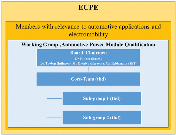 Fig. 4: ECPE Working Group [44]It can be seen that nano Ag and nano Cu are no longer the focus of technological variation. It can also be deduced that the process temperatures are in the moderate range, but that the warpage properties of the joining parts must be taken into account in order to minimize mechanical stresses in the module structure. The transition from Ag sintering to Cu sintering is characterized by the change in atmosphere from nitrogen to hydrogen. Overall, the parameters sintering pressure, sintering time and sintering temperature are very inconsistent and this raises the question of standardization, as otherwise published data on power cycle strength and thus module reliability are difficult to compare. The issues of standardizing processes, process parameters and test procedures for diagnosing module reliability require national and international cooperation, as is standard practice in surface mount technology today. The characteristics of incomplete standardization are also reflected in the inspection and test procedures(Fig. 6). The standardization activities in the automotive sector are presented in [44](Fig. 4 and 5).
High temperature storage
- 150 °C, 500 h
- 155 °C, 1000 h
- 200 °C, 1000 h, 3000 h
- >= 200 °C
- 25 °C to 250 °C
- 250 °C, 4 h, 250 h, 1000 h
- <= 300 °C
- 300 °C, 96 h, 512 h,
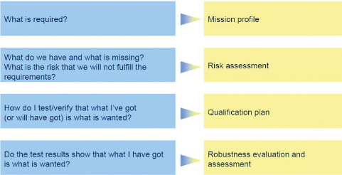 Fig. 5: Robustness validation in the...
 . ..automotive sector [44]
The temperatures used are very inconsistent. However, it is clear that the maximum temperatures follow the requirements for the high-temperature modules. It is important in this context that the thermal resistance of the module materials must meet new requirements. Here it can essentially be deduced that the thermomechanical properties are of particular importance. In particular, the efforts to further develop the substrate materials are recognizable here [67-75].
|
TCT -65/+150, 500cycles, HTS 175°C 1000h |
Yao, ECTC 2018 |
|
HTS 175 °C / 200 °C |
Cho, ECTC 2018 |
|
TCT -40/+150, 2500cycles |
Zhao, ECTC 2018 |
|
TCT -65/+150, 500cycles, AEC-Q100; HTS 300°C, 50-2000h |
Yang, ECTC 2018 |
|
TCT, HTS |
Chew, ECTC 2018 |
|
HTS 245, 273, 287°C; 72h, 336h |
Chiu, ECTC 2018 |
|
MIL-STD 883H, method 2019.8 |
Fu, ECTC 2018 |
|
HTS 175 °C, 1000h; TCT-40/+175, 1500cycles |
Guyneot, ECTC 2018 |
|
TCT-40/150, 250cycles |
Schiffmacher, ECTC 2019 |
|
TCT-40/200, 1000cycles |
Liu, ECTC 2019 |
|
TCT-50/200, 1000cycles; HTS 250 °C, 500h |
Tang, ECTC 2019 |
|
TCT-40/150, tdwell=1h to150 °C, transition 30sec to -40 |
Nijay, ECTC 2019 |
|
H3TRB, silicone potted Al2O3, dried 48h, 100 °C, followed by 85/85 |
Kolbinger, ECTC 2019 |
|
TCT-40/150 |
Sokolov, ESIME 2018 |
|
Thermo-mechanical non-linear FEM, 5 thermal cycles; elasticity, plasticity, CTE |
Solokov, ESIME 2018 |
|
Active and passive heating and cooling |
Kashko, ESIME 2018 |
|
Look-in-thermography (hot spots in power devices) |
Vellvehi, ESIME 2018 |
|
Cyclic cohesive zone model |
Springer, ESIME 2018 |
|
Multi-scale modeling Silvaco and Dmol3 software |
Zheng, ESIME 2018 |
|
Power cycling |
Jiang, ESIME 2018 |
|
Power cycling; electro-thermo-mechanical model |
Jiang, ESIME 2018 |
|
Power cycling +30/+180, 600,000cycles (LV124, LV324 for power electonics) |
Guyneot, ESIME 2018 |
|
FEM modeling of porosity in Ag sinter layer; 300 °C for 2000h |
Huang, ESIME 2018 |
|
Power cycling deltaT 80K, Tmin40°C, Tmax120°C |
|
|
Wagner, ESIME 2019 |
|
|
TCT -40/+175, 1500 cycles (PCB benzoxazine) |
Ratchev, EBL 2018 |
|
TCT +20 / +230 °C, 20cycles |
|
|
Kokash, ECTC 2017 |
|
|
HTS 200 °C, 750h |
Mavin curve, ECTC 2017 |
|
Power cycling test deltaT 140 °C, HTS 200 °C |
Feisst, ECTC 2017 |
|
HTS 175 °C, 3000h; TCT-50/150 °C, 2000cycles, JESD22-A104 |
Ueta, ECTC 2017 |
|
Power Cycling Test PCT3 |
Hutzler, ECTC 2014 |
|
TST -40/+175, -40/+200; 500 cycles |
Möller, ECTC 2014 |
|
TST -50/+150, 2000cycles |
Zhang, ECTC 2014 |
|
TCT -40/+200 and -55/+250 |
Xu, ECTC 2013 |
|
TCT-40/+200 °C at strain rates between 10exp-5 and 10exp-2 1/s. |
Herboth, ECTC 2019 |
|
TCT -40/+180; -40/+250, 750 (1000) cycles, (TSE11-A-S, ESPEC Corp.) |
Sakamoto, ECTC 2013 |
Fig. 6: Test and inspection procedures for sintered connections in power modules
Temperature Cycle Test
- +25/+250 °C
- -55/+90 (9300 cycles), 10 min each
- -40/+125, 1000 cycles
- -5/+200, 30 min each
- -55 °C/+150 °C, 1000 cycles
- -55 °C/+230 °C
- -40/+200 °C, 1000 cycles, 30 min each, 2000 cycles
- -40 °C/+250 °C, 1000 cycles
- -55 °C/+195, 1 min dwell
- > 300 °C
- 350 °C
The test conditions follow the requirements for the high-temperature modules, although the test conditions meet very different requirements. The highest test severity of -55 °C/+230 °C clearly shows that the extended thermal requirements for the module structure are decisive for corresponding technical reliability. Thermal shock or thermal cycling is not specified in every case, but is necessary for the results of the cyclic resistance.
Power Cycle Test
- Power Cycle Test
- deltaT 100K, 72 000 cycles, no-pressure sintering
- deltaT 130K, ton 1s
- 1500A, ton 15s, toff 15s
- deltaT 120K, 200 000 cycles
- deltaT 155K
- deltaT 165K
- deltaT 170K
- deltaT 130K
- deltaT 225K, 165 000 cycles, 200 000 cycles
- 180 000 cycles, ton 2s, toff 5s
- deltaT 100K, 17 000 cycles, 1 000 000 cycles
Similar to the thermal cycling tests, there is also a lack of consistency in the power cycle tests. Delta T values of up to 225 K also show the need for adapted module structures here. Up to 1,000,000 cycles at a deltaT of 100 K are described.
Toperating
- 250 °C
- 175 °C, 1000 A
- 220 °C
- 250 °C
- >=250 °C
Tjmax
- 250 °C
- 100 °C
- 175 °C, 800 A to 1000 A
- 200 °C
- >200 °C
- 230 °C
- 220 °C
- 250 °C
- >=250 °C
- deltaTj 100 K , heating, cooling 120 s
- High Humidity Test
- 1000 h, 85/85
- 500 h, 85/85
The high humidity test corresponds to the test conditions of the soldering modules and is also used here to analyze the corrosive resistance [76], influenced by the variance of the module materials. The results of the corrosive properties of the power module are shown in Table 1 from [76].
|
Substrate technology |
Insulating dielectric material |
Metali-zation |
Coating of the metali-zation |
Optional dendritic growth and time for different fluids |
||||
|
Tap water |
Deionized water |
Di water with H2SO4 |
Di water with HCI |
|||||
|
1 |
DBC |
AlN |
Cu |
- |
Yes, > 11 min |
Yes, > 5 min |
Yes, > 3 min |
Yes, > 1 min |
|
2 |
DBC |
Al2O3 |
Cu |
- |
Yes, > 10 min |
Yes, > 5 min |
Yes, ~ 1 min |
Yes, ~ 1 min |
|
3 |
DBC |
AlN |
Cu |
Ag |
Yes, > 1 min |
Yes, > 3 min |
Yes, ~ 1 min |
Yes, > 1 min |
|
4 |
DBC |
Al2O3 |
Cu |
Ag |
Yes, > 4 min |
Yes |
Yes, ~ 1 min |
Yes, ~ 1 min |
|
5 |
DBC |
AlN |
Cu |
Au |
No |
No |
Yes |
No |
|
6 |
AlSi soldered |
Al2O3 |
Al |
Ni |
No |
No |
No, but surface corrosion |
No, but surface corrosion |
|
7 |
IMS |
Al2O3 filled expoxy |
Cu |
Ag |
Yes |
Yes |
Yes, ~ 1 min |
Yes, ~ 1 min |
|
8 |
DBA direct casting |
AlN |
Al |
Ni |
No, but surface corrosion |
No, but surface corrosion |
No, but surface corrosion |
No, but surface corrosion |
|
9 |
AMB CuAgTi solder |
Si3N4 |
Cu |
Ni |
No, but surface corrosion |
No |
Yes, > 4 min |
Yes, > 2 min |
Table 1: DCB, DBA, AMB and IMS substrates with corresponding corrosion parameters [76]
Industry Standard Tests - Reliability
The test conditions (TCT, HTS, H3TRB, number of cycles or hours) resulting from the research are listed below. The most critical test condition with -55/+250 once again illustrates the importance of the functional materials in the module structure. All the TCT conditions listed below are very different in the deltaT of the absolute temperature. Standardization fails more due to the fact that the modules are equipped with very different functional materials.
In the interests of comparability of the test severity parameters achieved, it is essential to standardize the test parameters in order to achieve industry standards.
Cu sintering technology
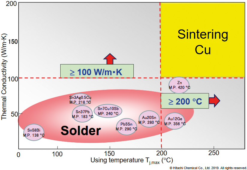 Fig. 7: Cu sintering technology[49]Cu sintering technology is equivalent to Ag sintering technology [66](Fig. 7 [49]). Differences arise in the choice of atmosphere for the sintering technology. Further integration technologies for power modules are presented in the area of chip embedding [47, 51-57, 66] and multilayer technology [48, 50, 58, 62, 63]. Below are some key features of the technology variations [46, 47]. Information on porosity as a function of the sintering pressure, the sintering temperature and the sintering atmosphere is given in [48](Fig. 8). Here, low pressure compounds are compared with each other. The extent to which low pressure sintering prevails for the C-sintered compounds depends on the porosity and the achievable shear strengths(Fig. 9). Here, the hydrogen content in the nitrogen atmosphere is a parameter when specifying the shear strengths.
Chip embedding
Embedding technology is one of the innovative chip-mounting technologies for power modules. Chip embedding technology has great potential in terms of cost, electrical performance, compactness and reliability. The degree of miniaturization is a constant requirement in microelectronics packaging. This also applies to the field of power modules, where SiPs in particular represent a module type with high variables in packaging technology. The integration of components into the printed circuit board material (known as PCB embedding) has enormous advantages in the production and connection technology of power modules and has great benefits from various aspects. Firstly, the PCB embedding technology and the thick copper substrates increase the thermal performance, secondly, the package construction leads to smaller package parasitics. Consequently, the switching losses are also reduced. This, in combination with lower thermal impedance, increases the power density at system level. Furthermore, this technology has the potential for cost effective manufacturing with PCB board level capabilities.
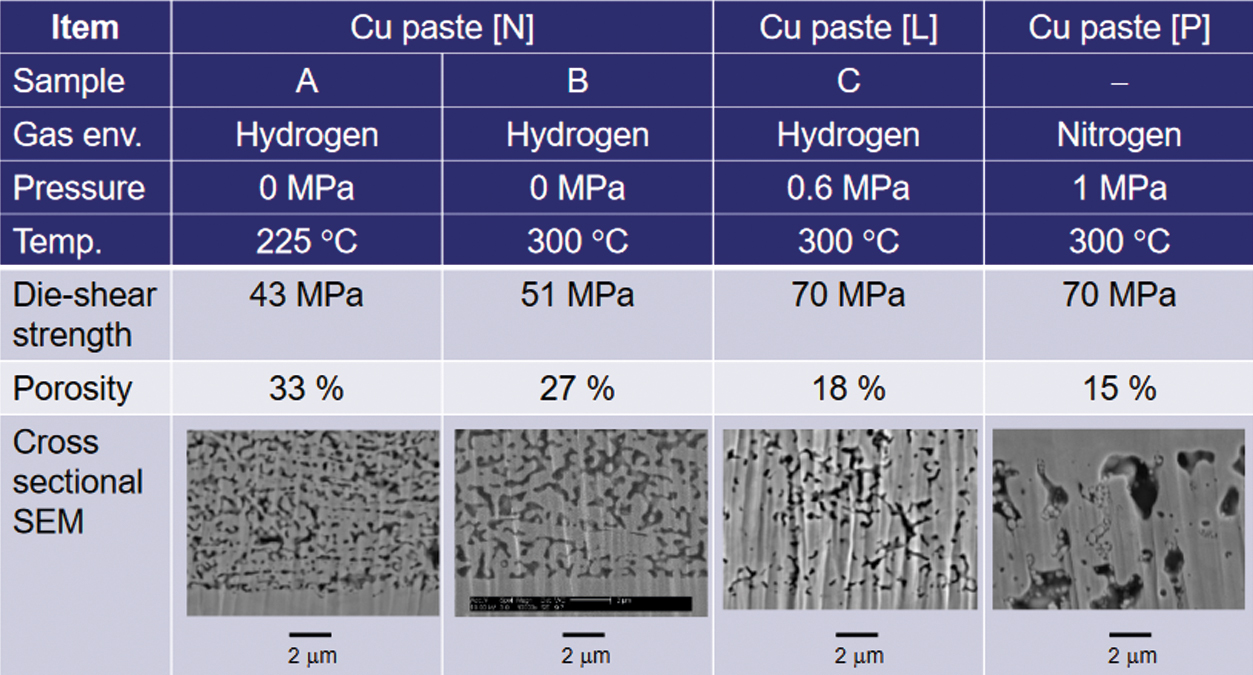 Fig. 8: Porosity of Cu sintered interconnects [49]
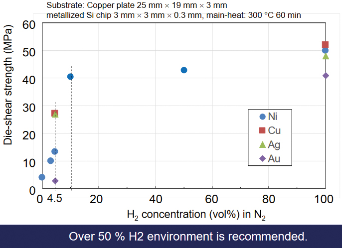 Fig. 9: Die shear strength of Cu sintered interconnects on different metallizations of the substrates [49]
With regard to the increasing demands on miniaturization, the power loss density increases, which makes thermal management more difficult. One way of minimizing the influence is PCB embedding of the semiconductors. This approach leads to shorter thermal paths from the semiconductor to the heat sink compared to the established DCB module technology. The production of embedded modules with established embedding processes leads to dielectric cooling capability. The PCB embedded package in Figure 10, has a size of 10 x 10 mm [77] and is based on the ECPTM technology from AT&S. The X-ray image(Fig. 10b) shows the layout. Micro-vias are used here as an intermediate connection technology between the chip metallization and the Cu layers on the top and bottom sides.
 Fig. 10: Schematic layout and PCB embedded power device (The semiconductors are mounted onto a thick copper leadframe, which is embed-ded into a PCB by adhesive bonding) [59, 77]
 Source: Hitachi Chemical Co, Ltd. 2019
The micro-vias are used for electrical as well as thermal connection, and the through-vias can also be used for the connection between the top and bottom side of approx. 3.5 K/W and a thermal resistance of approx. 17 K/W on the top side [77]. PCB embedding technology requires the substrate material to be in a good ratio to the semiconductor from the CTE point of view [61] in order to reduce local stress. Efforts are being made to develop and apply new types of substrates [60].
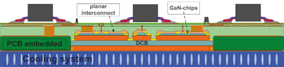 Fig. 11: Planar packaging technology [47]
Outlook
Part 2 of this article will appear in PLUS 11/2020 and will deal with questions on technology variants, the testing philosophy, non-destructive testing, FEM simulations for CTE matching, the results of power cycling and the reliability assessment under accelerated tests.
The following focal points, which have been identified as technology variants and influencing factors in the area of 'Materials for Technology for Power Electronics', are explained in more detail in Part 2:
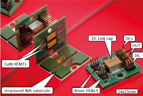
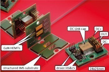 Fig. 12: PCB embedded chip assembly [1]Directional Solidification of Soldered Power Modules
- Ag sintering
- The Transfer Film
- Ultrasonic Assisted Sintering
- Laser Assisted Sintering
- Infrared Assisted Sintering
- The Top System
- Cu Sintering
- TLP Bonding
- SLID Bonding
- Embedded Power Electronics
- Additive Manufacturing of Power Electronics
- Direct Pressed Die Technology
- Wafer Level 3D Power Integration
- Bond Buffer
- Substrates
- Plasma Coating
- Stacked Ceramics / Modules
- Cooling
- Electrochemical Corrosion
- Non-destructive Testing
- Power Cycling
- H3TRB Test
- Transient Thermal Analysis
- Encapsulation
- Ribbon Bonding
- Lifetime Ceramic Capacitor
- FEM for Power Electronics
- Tests Sinter Interconnects
- Industry Standard Tests-Reliability
www.avt.et.tu-dresden.de, www.budatec.de
References
[1] Klein: Power module design for utilizing of WBG switching performance PCIM 2019
[2] BLEY: The Interconnection for Power Module 3.0 ECPE 2019
[3] Mitamura: A transfer-molded high temperature SiC power module withstanding up to 250 °C CIPS 2018
[4] Rittner: Innovative Reliable Nitride based Power Devices and Applications -The EU Public Funded Project 'InRel-NPower2018
[5] Huber: Novel SiC Module Design - Optimized for Low Switching Losses,Efficient Cooling Path and Low Inductance CIPS 2018
[6] Blank: Low Temperature Silver Sinter Processes on (EN)EPEAg Surfaces for High Temperature SiC Power Modules CIPS 2018
[7] KIM: Pressure-less nano silver bonds for liquid cooled IGBT modules CIPS 2018
[8] Takemasa: Die-bonding performance of micron Ag particle paste for high power devices CIPS 2018
[9] Chew: Silver sinter paste optimized for pressure sintering under air atmos-phere on precious and non-precious metal surfaces with high reliable sintered joints CIPS 2018
[10] Rudzki: Evolution of Sinter Paste ECPE 2019
[11] De Monchy: New Sintering Form Factors for Next Generation Power Modules ECPE 2019
[12] Schmitt: Pressureless sintering of large dies by infrared radiation CIPS 2018
[13] Guo-Quan Lu: Advanced Die-attach by Metal-powder Sintering: The Science and Practice CIPS 2018
[14] Waltrich: Highly reliable power modules by pressureless sintering CIPS 2018
[15] Chew: Direct bonding to aluminum and nickel surfaces by pressure silver sintering PCIM 2019
[16] Watanabe: Stable Microstructure and Mechanical Properties of Pressureless Sintered Silver at a Temperature of 250 ºC PCIM 2019
[17] Inoue: Design of Interfacial Chemistry for Inducing Low Temperature Sintering of Silver Micro-fillers within Epoxy-based Binders EMPC 2019
[18] Nishikawa: Effect of bonding temperature on shear strength of joints using micro-sized Ag particles for high temperature packaging technology EMPC 2019
[19] Stojek: Metalization impact on heat transfer through sintered nanosilver based thermal joints EMPC 2019
[20] Ueshima: Ag and Si particles sintering technology for SiC EMPC 2019
[21] Gökdeniz: Behavior of Silver-Sintered Joints by Cyclic Mechanical Loading and Influence of Temperature EMPC 2019
[22] Schwarzer: Pressureless Sintering on Plasma based Cu metallizations EMPC 2019
[23] Nakako: Sintered Cu bonding pastes and their bonding reliabilities ECPE 2019
[24] Yasui: A 3.3kV 1000A High Power Density SiC Power Module with Sintered Copper Die Attach Technology PCIM 2019
[25] Nakako: Relationship Between Bonding Properties and Porosity of Sintered Cu Bonding PCIM 2019
[26] Yamauchi: The characteristics of Sintered Copper Layer by Pressure Sintering Process for Power Module Application PCIM 2019
[27] Takata: Sintering Cu Paste on Cu Plates with Different Metallization PCIM 2019
[28] Gao: Highly Reliable Package using Cu Particles Sinter Paste for Next Generation Power Devices PCIM 2019
[29] Stenzel: Alternative sinter materials for power electronic EMPC 2019
[30] Del Carro: Sintering of oxide-free copper pastes for the attachment of SiC power devices EMPC 2019
[31] Reinhardt: PrintPOWER - Paste systems for multifunctional copper power modules EMPC 2019
[32] Hlina: Advanced Application Capabilities of Thick Printed Copper Technology EMPC 2019
[33] Feißt: Power Chip Interconnections Based on TLP and Sintering of CTE-Matched Conductors CIPS 2018
[34] Guo-Quan Lu: Advanced Die-attach by Metal-powder Sintering: The Science and Practice CIPS 2018
[35] Bhogaraju: Hybrid Cu particle paste with surface-modified particles for high temperature packaging EMPC 2019
[36] Del Carro: Sintering of oxide-free copper pastes for the attachment of SiC power devices EMPC 2019
[37] Polezhaev: Development of a novel 600V[50A power package with semiconductor chips sandwiched between PCB substrates using double-side Ag-sintering PCIM 2019
[38] Streibel: Reliability of SiC MOSFET with Danfoss Bond Buffer Technology in Automotive Traction Power Modules PCIM 2019
[39] Abe: Dielectric Properties and Partial Discharge Inception Voltage of Aluminum Nitride Insulating Substrate at High Temperatures CIPS 2018
[40] Mitamura: A transfer-molded high temperature SiC power module withstanding up to 250 °C CIPS 2018
[41] Johnson:10 kV SiC Power Module Packaging CIPS 2018
[42] Müller : Selective Silver Sintering on Organic-Based Circuit Boards PCIM 2019
[43] Liu: High temperature wireless packaging of SiC power device by organic-free die-attach material sintering PCIM 2019
[44] Rittner: Automotive Qualification Routines for Power Electronics Components in Electrified Powertrains CIPS 2018
[45] IDAKA: New Developments in Resin Encapsulated Power Module ECPE 2019
[46] Mitamura: A transfer-molded high temperature SiC power module withstanding up to 250 °C CIPS 2018
[47] Rittner: Innovative Reliable Nitride based Power Devices and Applications -The EU Public Funded Project 'InRel-NPower2018
[48] Welker: Power System in Package based on Multilayer Ceramic Substrates ECPE 2019
[49] Nakako: Sintered Cu bonding pastes and their bonding reliabilities ECPE 2019
[50] Yamauchi: The characteristics of Sintered Copper Layer by Pressure Sintering Process for Power Module Application PCIM 2019
[51] Schnur: Design and Fabrication of PCB Embedded Power Module with Integrated Heat Exchanger for Dielectric Coolant CIPS 2018
[52] Bach: Vias in DBC Substrates for Embedded Power Modules CIPS 2018
[53] Reiner: PCB Embedding for GaN-on-Si Power Devices and ICs CIPS 2018
[54] Yang: Comparison of thermal and reliability performance between a SiC MOSFET module with embedded decoupling capacitors and commercial Si IGBT power modules CIPS 2018
[55] Bach: Ceramic Embedding Technologies for High Temperature Power Electronics ECPE 2019
[56] Schweizer Electronic: 60% Performance Increase by Power MOSFET Embedding ECPE 2019
[57] Polezhaev: Development of a novel 600V/50A power package with semiconductor chips sandwiched between PCB substrates using double-side Ag-sintering PCIM 2019
[58] Bach: Vias in DBC Substrates for Embedded Power Modules CIPS 2018
[59] Reiner: PCB Embedding for GaN-on-Si Power Devices and ICs CIPS 2018
[60] Mitamura: A transfer-molded high temperature SiC power module withstanding up to 250 °C CIPS 2018
[61] Müller: Selective Silver Sintering on Organic-Based Circuit Boards PCIM 2019
[62] Mouawad: On the reliability of stacked metallized ceramic substrates under ther-mal cycling CIPS 2018
[63] Welker: Power System in Package based on Multilayer Ceramic Substrates ECPE 2019
[64] Chew:Silver sinter paste optimized for pressure sintering under air atmosphere on precious and non-precious metal surfaces with high reliable sintered joints CIPS 2018
[65] Chew: Direct bonding to aluminum and nickel surfaces by pressure silver sintering PCIM 2019
[66] Bhogaraju: Hybrid Cu particle paste with surface-modified particles for high temperature packaging EMPC 2019
[67] Bach: Ceramic Embedding Technologies for High Temperature Power Electronics ECPE 2019
[68] Abe: Dielectric Properties and Partial Discharge Inception Voltage of Aluminum Nitride Insulating Substrate at High Temperatures CIPS 2018
[69] Mitamura: A transfer-molded high temperature SiC power module withstanding up to 250 °C CIPS 2018
[70] Johnson:10 kV SiC Power Module Packaging CIPS 2018
[71] Welker: On the Thermal Performance of Si3N4-Based Ceramic Multilayer Substrates PCIM 2019
[72] Kwak: The thermal and mechanical properties of reinforced AlN with metal bonding types PCIM 2019
[73] Müller: Selective Silver Sintering on Organic-Based Circuit Boards PCIM 2019
[74] Liu: High temperature wireless packaging of SiC power device by organic-free die-attach material sintering PCIM 2019
[75] Bao Ngoc: A Novel Double Sided Cooled Leadframe Power Module for Automotive Application based on ceramic-free Substrates CIPS 2018
[76] Bayer: Electrochemical Corrosion on Ceramic Substrates for PowerElectronics - Causes, Phenomenological Description, and Outlook CIPS 2018
[77] Schnur: Design and Fabrication of PCB Embedded Power Module with Integrated Heat Exchanger for Dielectric Coolant CIPS 2018
[78] Mitamura: A transfer-molded high temperature SiC power module withstanding up to 250 °C CIPS 2018
[79] Takemasa: A transfer-molded high temperature SiC power module withstanding up to 250 °C CIPS 2018
