In Part 1 of the overview article on joining processes from the sintering technology sector used in electronics production (PLUS 10[2020, p. 1353 ff), the sintering process itself was primarily explained. Here in Part 2, recognizable trends and technological features are examined and evaluated in more detail in order to record the influencing factors on the process technology and ultimately on the reliability of the high-temperature-suitable joining technology. It also deals with technology variants.
Part 1 of this overview article on joining processes from the technology area of sintering used in electronics manufacturing (PLUS 10[2020, p. 1353 ff), above all explains the sintering process itself. Part 2 evaluates visible trends and technological features in detail to determine the influencing variables on the process technology and examines the reliability of the joining technology suitable for high temperatures. In addition, it also deals with technology variants.
|
Macro-voids |
Biggest voids in solder layers due to wetting issues |
|
Planar micro-voids |
Small voids due to inclusions |
|
Shrinkage voids |
Occur during solidification |
|
IMC micro-voids |
Occur within intermetallic phases |
Tab. 1: Void types in the soldering plane [1]
Technology variants
The following focal points have been identified as technology variants and influencing variables:
Directional Solidification of Soldered Power Modules
In [1], this technology is described as a process for reducing the void rate and increasing reliability by using the DSM process (Directional Solidification Mechanism). Special pins control the heat flow in the heating and cooling phase to significantly reduce shrinkage voids in the solder plane.
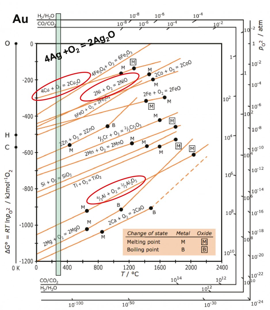 Fig. 1: Ellingham-Richardsson diagram with standard free energy of formation of metal oxides [6]
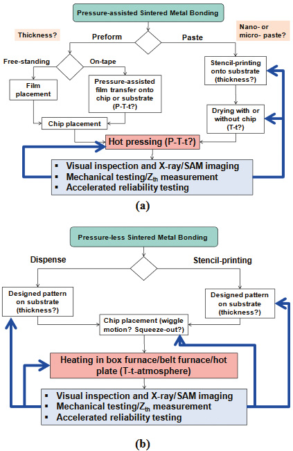 Fig. 2: Flow chart for pressurized (a) and unpressurized (b) sintering processes [6]
Ag sintering
Ag sintering as a process for the production of compounds suitable for high temperatures is described in [2, 44, 54, 61, 64, 65, 67, 88]. The features of joint formation under the differentiated technological approaches, which decisively characterize the reliability of the joints, are listed here. Compared to conventional soldered joints, Ag sintered joints have more than 5 times the thermal and electrical conductivity [6]. When a chip is fixed to the substrate with the sintering paste, the number of metal particles that are physically in contact with the solids depends on many factors: the applied pressure, the particle size distribution, the surface roughness, the oxide-free nature of the sintered particles [6] and the wetting characteristics of the organic molecules in the sintering paste. The freedom from oxides(Fig. 1) can be calculated according to [6]. Figure 2 shows a flow chart for the production of pressurized and unpressurized sintered compounds [6], the differences of which can be seen in the drying phase and the application of the printing component.
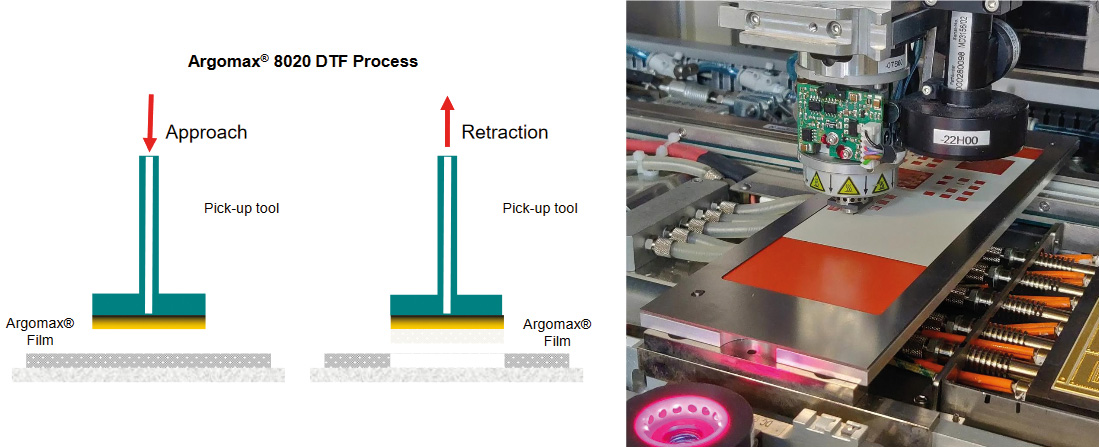
 Fig. 3: The transfer film and wafer-oriented process flow [3]
The transfer film
3] shows how a prefabricated die transfer film supports the formation of the interconnection without sintering paste printing(Fig. 3). The die transfer film is picked up in the placement process with the die and the die geometry and placed on the substrate for joint formation by sintering.
Ultrasonic assisted sintering
The ultrasonic assisted joining process makes targeted use of horizontal or vertical ultrasonic transfer to stabilize the joint formation in the sinter paste-controlled assembly. This allows the pressure component to be reduced, thus leading to mechanical relief of the die in the sintering process in the case of pressurized sintering.
Laser assisted sintering
4] describes how the process is energetically supported during wire or ribbon bonding in order to increase the quality of the bond formation.
Infrared assisted sintering
The production of the sintered joint is described for pressureless sintering processes [5, 72] and is supported here by targeted infrared radiation. Using typical sintering profiles(Fig. 4), pressureless sintering is effectively supported by superimposing infrared radiation(Fig. 5). Sintering processes with infrared radiation are already known from printed electronics.
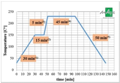 Fig. 4: Typical sintering profile [5]
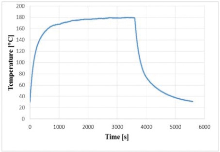 Fig. 5: IR sintering profile [5]
Z. E.g. sintering of Ag inks on RFID cards, which are used as part of telephone or credit cards as copy protection or as a security feature in ID cards. Infrared light is defined for wavelengths from 0.4 to 5 µm. IR radiation is used in the manufacture of electronic circuits by IR soldering or for drying materials. Infrared radiation is divided into three categories, short, medium and long wave. A wavelength of 0.78 to 1.4 µm is used for sintering silver [5].
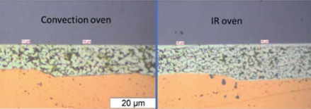 Fig. 6: Cross-section of a sintered joint in a convection furnace (left) and IR furnace (right) [5]A shear strength of 10 MPa was observed after 30 minutes of sintering with IT radiation. This is the minimum shear strength that ensures reliable connections between chip and substrate [5].Figure 6 shows joining planes of sintered joints after processing in a convection oven and an IR oven. Void-free interfaces were achieved after IR processing.
The Top System
The die top system shows a Cu structure on the top side of the chip, is sintered and is the joining partner of the thick Cu wire assembly(Fig. 7) [7]. The sintered copper structure on the top side of the chip is the characteristic feature of the connection structure to increase the reliability of the power modules.Figure 8 shows the schematic process flow of the die top technology.
Cu sintering
A very comprehensive description of Cu sintering technology, which is carried out in a hydrogen atmosphere, can be found in [8, 32, 40, 42, 45, 46, 48, 63, 64, 66, 108, 111]. Here, pressurized and unpressurized Cu sintering is described (see also Part 1). As tabulated in Part 1, the drying time of the Cu sintering paste, the sintering pressure and the sintering time are varied. The main difference to Ag sintering is the sintering atmosphere used. Cu sintering is carried out in a hydrogen atmosphere in order to reduce passive layers. Cu sintering is a precious metal-free joining technique.
In the following, TLP and SlID bonding are explained as an alternative for the production of high-temperature-suitable connections for power electronics, as formulated in the introduction.
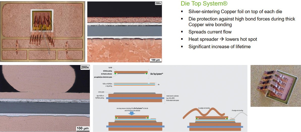 Fig. 7: The top system [7]
TLP Bonding
A detailed description of TLP (Transient Liquid Phase Bonding) is given in [9, 10]. TLP bonding with Cu/Sn or Ag/Sn multilayers is verified as a bonding method for high temperature power electronics. Ag and Sn layers with a content of 72 vol. % silver are required. Isothermal solidification above the melting point of Sn results in Ag3Sn phases. Isothermal solidification above the melting point of Sn results in the Ag3Snphase, which is stable up to 480 °C. To avoid oxidation in the bonding process, the process can be carried out under vacuum. A bonding pressure of 5 MPa is recommended for good interface quality.
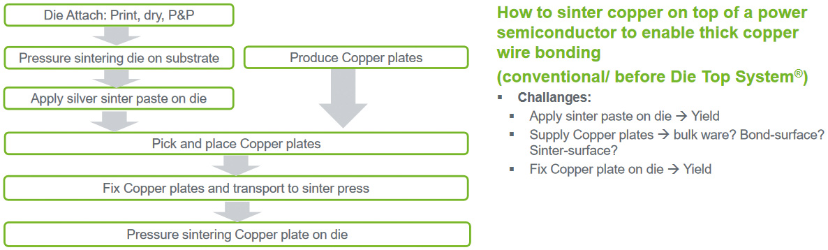 Fig. 8: Process flow of the Die Top technology [7]
Cu-Invar-Cu composite material is well known as a core material for special PCBs. The Invar core is coated with Cu on both sides with a total thickness of 150 μm. The layer ratio is 12.5/75/12.5 vol. % with a 112.5 μm core with 2 x 18.75 μm Cu. The lower CTE value is known and advantageous in terms of reliability. Transient liquid phase bonding with Ag/Sn is one of the advantageous solutions.
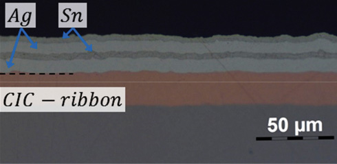 Fig. 9: Electroplated Ag/Sn multilayer on Cu-Invar-Cu for TLP bonding [9]
 Fig 10: Schematic representation of an embedded power module. IGBT is mounted on a Cu substrate and embedded in a PCB [96]
For the Cu/Sn combination, the application can be used on DCB substrates with a special layer stack of Cu and Sn. This supports the transformation of the solder joint to the more stable Cu3Sn phase. Optimized Cu/Sn layer stacks make the joint more reliable through TLP bonding (TLPB) with formed intermetallic phases for the permanent solder joint. In general, the performance of the joint can be increased by TLPB. The process is easy to implement in industrial soldering systems as a standard process. Joints with an application above 300 °C are possible.
 Fig 11: PCB embedding of WBG semiconductors [97]
 Fig 12: Cross-section of a demonstrator module [98]
SLID bonding
The process description is contained in [11, 28, 29, 62]. Au/Sn SLID bonding (Solid Liquid Interdiffusion) has been specially developed for harsh environment applications. Solid-liquid interdiffusion (SLID) bonding is a technique based on binary or ternary (Au-In-Bi) systems that form high-temperature stable intermetallic phases at moderate bonding temperatures [18]. Cu|Sn [12-14] and Au|Sn [15-17] are the most studied SLID systems with process temperatures of 232 °C and 278 °C, and with intermetallic phases with melting temperatures of 700 °C and 500 °C, respectively. The moderate bonding temperatures of the SLID process also enable joining technology for thermally sensitive joining parts. Heating from RT to 250 °C and maintaining the temperature for a few minutes leads to heating of the air humidity and ensures that the temperature is maintained for uniform temperature distribution. Bonding is achieved by solid-state diffusion and subsequent growth of the intermetallic phases [13].
Embedded power electronics
3D embedding is described in [52]. As a result of the increasing demands for miniaturization of power modules and the significant increase in power loss, thermal management is becoming difficult. One way to circumvent this fact is PCB embedding of semiconductors [78, 79, 81, 92, 93, 96, 97, 98, 112]. A schematic diagram from [96] shows the integration structure of embedding technology. PCB embedding offers the following advantages [98, 99]:
a. Embedding significantly reduces the module volume, no package is required
b. Miniaturization reduces parasitics (resistance, inductance)
c. Improved thermal impedance due to thick Cu substrates for heat spreading; panel level manufacturing reduces production costs.
 Fig 13: Cross section of a sintered semiconductor on printed circuit board with optimized sintering parameters (3.8MPa, 210s, 200oC) [100]The power semiconductors are sintered as bare die with the Cu conductors on the top side. The final module is produced by simultaneous sintering with an Ag paste for the electrical contacts and an FR4 prepreg for the mechanical support. Further developed sintering pastes allow the process temperature(Fig. 13) and the process pressure to be reduced. New high-temperature stable resins of the PCB material with Tg values of approx. 200 °C also ensure thermal performance.
Additive manufacturing of power electronics
The technology variant is presented in [95]. Plasma spraying enables the coating of material combinations with the deposited process sequence. This is a variant of substrate metallization for the sintering process.
Direct Pressed Die Technology
DPD technology (direct pressed die technology) is the combination of double-sided sintered dies with a direct printing system on top of each power semiconductor [26, 80]. Silicone elastomers have special properties such as high and low temperature stability (-40°C to 200°C) over a long period of time, excellent electrical behavior as well as a breakdown field strength of 23 kV/mm, CTI values of 600 and meet additive requirements for compression stability up to 200 °C. The basic design is shown in [94](Fig. 14).
 Fig. 14: Basic design of DPD technology [94]
These modules consist of substrates, dies and a printing system and can be applied multivalently. This technology can fulfill the performance and thermal cycle stability requirements of power modules up to the required values of the new application. The confidence level for DPD technology is 200,000 power cycles with deltaT = 110K (IEC 60749-34) [94].
Wafer Level 3D Power Integration
Wafer Level3D Power Integration is a new path towards power systems. For example, in the EU project ENIAC JU 'Enhanced Power Pilot Line (EPPL)', new structures of wafer level components are being developed and investigated in order to integrate lateral power components in Si interposers. 3D integration will gain importance, just as the technology has found its way into smartphones. 3D integration provides short contacts with low parasitic effects and improves energy efficiency through innovative solutions. The increasing demands on the performance, reliability and cost-effectiveness of electrical power systems can be achieved through the development of integrated systems and modules. Based on the co-integration of semiconductor components and WBG structures with integration-capable features, standardized interfaces, production-capable processes and a wide range of applications can be achieved. The high currents necessary for the application require electrical resistors between the transistors that are as small as possible. Furthermore, the distance between the driver and the power components must be reduced in order to achieve the highest switching frequency. The global architecture of modules is described in [20, 21, 74].
 Fig. 15: Schematic Si interposer technology [30]
 Fig. 16: Cross-section of integrated module structure [30]
 Fig. 17: SEM image of a Cu nanoparticle layer after the sintering process with 43 % porosity [74]
Metal pastes based on nanoparticles [74] offer the possibility of significantly reducing the temperature during sintering compared to bulk materials [16]. The reduction of the sintering temperature with the reduced particle size is associated with an increase in the surface energy. Nano-Cu pastes offer the advantage of low-temperature processes with the combination of variable chip metallization.
Wafer level 3D technology provides an effective pathway for integrated power systems [83]. In the EU project EPPL, new types of modules based on Si interposers were developed and investigated.
Bond Buffer
The technology is presented in [22, 23, 27, 38, 39]. The top system technology [24, 25, 37] is related.
Substrates
The most commonly used materials are ceramic materials Al2O3, AlN, Si3N4, GaN and LTCC(Tables 2 and 3). Si3N4 is used for multilayer substrates and combines high fracture toughness with high thermal conductivity [110]. The ceramic is not oxide-based and is suitable for layer stacks. The complete layer stack of the substrate is produced in one brazing step. Si3N4 can withstand the required number of thermal cycles due to its mechanical design. Furthermore, the deflection can be reduced, which is particularly important for the die attach. The deflection of the substrate is the result of the different expansion coefficients of the ceramic layers and the copper layers. The mismatch of the CTE values causes mechanical stress in the substrate [31]. Due to the required cooling performance and hot spot management, Si3N4 is the preferred concept for Si3N4-AMB (Active Metal Brazing) [78].
|
Property |
unit |
Al2O3 |
AlN |
Si3N4 |
|
Thermal Conductivity |
W/(m-K) |
20-30 |
70-250 |
60-90 |
|
Dielectric Strength |
kV/mm |
>12 |
>14 |
>14 |
|
Relative Dielectric Constant at 20 °C |
- |
9-10 |
8-9 |
7-9 |
Table 2: Properties of ceramic substrates [89]
|
Material |
Density (kg/m3) |
CTE (K) |
Thermal Conductivity (W/mK) |
Young's Modulus (GPa) |
Poisson's Ratio |
|
GaN |
6100 |
5,6 x 10⁻⁶ |
110 |
181 |
0,352 |
|
Ag paste |
6294 |
19 x 10-6 |
430 |
12,9 |
0,1 |
|
SAC305 |
7400 |
23,5 x 10⁻⁶ |
64,2 |
54,2 |
0,35 |
|
Sn Ag Sb Cu |
7300 |
24 x 10-6 |
41,6 |
46,2 |
0,3 |
|
Au |
19 300 |
14 x 10-6 |
320 |
78 |
0,3 |
|
Cu |
8300 |
16,5 x 10⁻⁶ |
401 |
110 |
0,34 |
|
Si3N4 |
3270 |
3,2 x 10⁻⁶ |
80 |
310 |
0,24 |
High Tg prepregs continue to be used as organic substrates as described in [34, 35]. The general advantages are discussed for PCB embedding in [34, 35]. The glass transition temperature is also essential because the CTE value is strongly dependent on the temperature range after the Tg value. For example, a resin with a Tg value of 270 °C was developed in [90].
Combinations of FR4 and AlN [41] and Si3N4 substrates sintered on AlSiC baseplates [47, 49] are also known.
IMS substrates [55, 56] and Cu leadframe materials are also used as substrates [58], as is LTCC as a substrate material [59, 60, 78]. Silver sintering on ceramic carriers is used in mass production. Sintering on standard PCBs is a niche application. High-temperature multilayer printed circuit boards are under development or can be seen in initial applications [92].
In [34, 92, 93] a solution for PCB embedding (Heterogeneous Integration of a Power SiP) is presented(Fig. 18). A power system in package based on IMS substrates is described in [126].
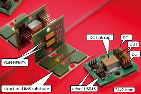 Fig. 18: GaN InPM. PCB Embedded / IMS integrated link and driver [93]
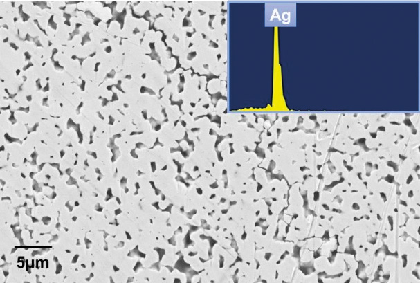 Fig. 19: Cross-section through an organic-free Ag layer [68
Plasma coating
Organic-free layers are deposited on substrates using the PLD technique (plasma-based coating method). The surfaces are cleaned using citric acid, acetone and ethanol to remove the impurities before plasma coating. The ultrafast laser ablates the Ag target and coats the substrate. The thickness of the deposited Ag layer is determined by the controlled PLD process.
After the PLD process, the organic-free Ag layer is sintered and forms the structure as shown in Figure 19. Compared with paste-based sintering technology, the sintered layer is denser and has good interfacial properties. The porosity of the sintered organic-free layers is around 16 %. The lower porosity improves the electrical and thermal conductivity.
The publication [71] investigates the interaction of a Cu interface, produced by additive metallization, on ceramic substrates by the plasma coat process and the compound formation in a pressureless sintering process. This method shows the potential of Cu metallization on semiconductors to realize the Cu bonding process on functional materials [71].
Stacked ceramics/modules
Two stacked substrates, AlN based stack on DCB substrates and Si3N4 based stack on AMB substrates, are presented in [102, 103]. Cross sections of these stacks are shown in Figure 20.
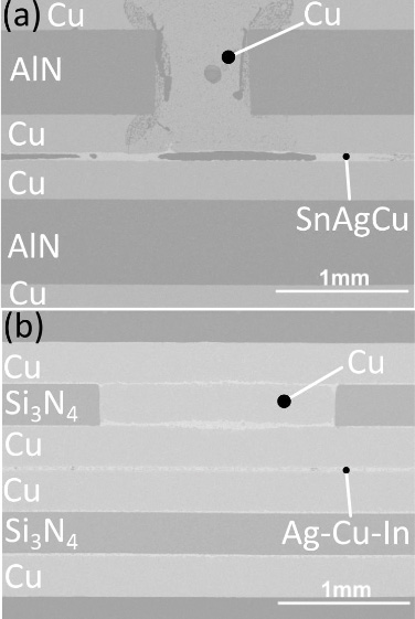 Fig. 20: SEM images of the two samples a) Sample A, b) Sample B. The Cu-filled vias are also recognizable [102]
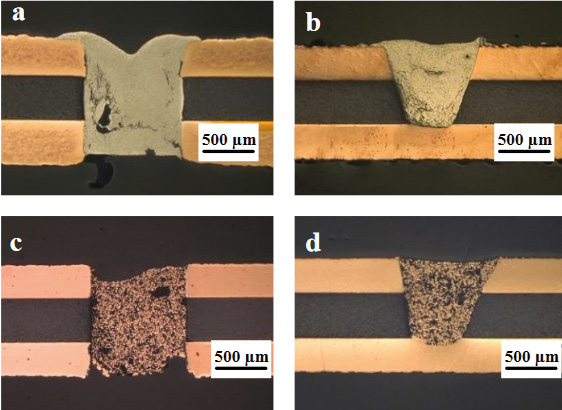 Fig. 21: Cross-sections of vias in DBC after dispensing and sintering a) b) silver paste; c) d) Cu paste [104]
In the case of Si3N4 based stacked AMB substrates, no lifting of the Cu layer was observed. TCT -55/+195 provides stable bonds up to 3000 cycles. however, cracks were detected at the corners of the ceramic. The procedural possibilities of vias in DBC are characterized in [104].
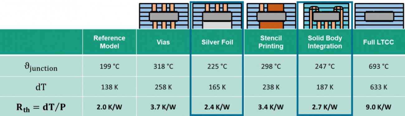 Fig. 22: Technological variants of LTCC embedding up to the full LTC package [106]
In addition to the stacked variants described, the material-specific approach of LTCC embedding is presented in [106].
Electrochemical corrosion
The corrosive stability/instability is presented in [105]. Table 4 provides an overview of the corrosive properties of DCB structures in comparison with IMS and AMB substrates and illustrates, among other things, the risk of dendrite formation, which can lead to module failure.
Power cycling
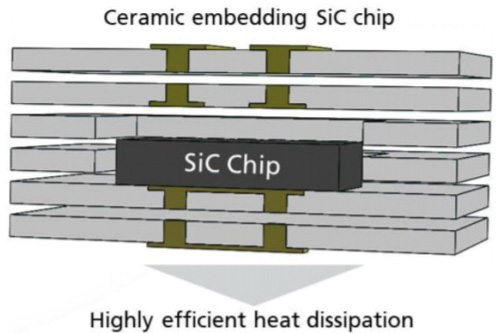 Fig. 23: Full LTCC package for junction temperatures up to 400 °C [106]The power losses in power modules induce vertical and horizontal temperature gradients in the layer stack between the WBG semiconductor and the cooling, which generates mechanical stress in the layers and the junction level [115]. This stress causes ageing processes and cumulative damage and leads to faults in the power module. In particular, the material-specific differences in the CTE value are responsible for service life restrictions in the application. Conversely, this would mean that coating systems with comparable CTE values do not generate mechanical stress under functional conditions. However, taking the vertical and horizontal temperature gradients into account, mechanical stress can also be expected here. These temperature gradients together with the different losses as a function of time make it impossible to design a power module without limitations in the service life. Depending on the thermo-mechanical stress, the defined operating conditions are a component of the power module.
An extension of the temperature range requires an increase in service life under the conditions of thermo-mechanical stress [75]. Active power cycle tests allow the prediction of the service life of power modules under thermo-mechanical stress resulting from the application-specific stresses [75]. Depending on the power cycling test parameters, such as pulse duration, power level, deltaT, ton and toff and cooling conditions, a variety of defects and degradation mechanisms become effective during the cycles and influence the thermo-mechanical stress from the semiconductor to the cooling interface [77, 101, 115].
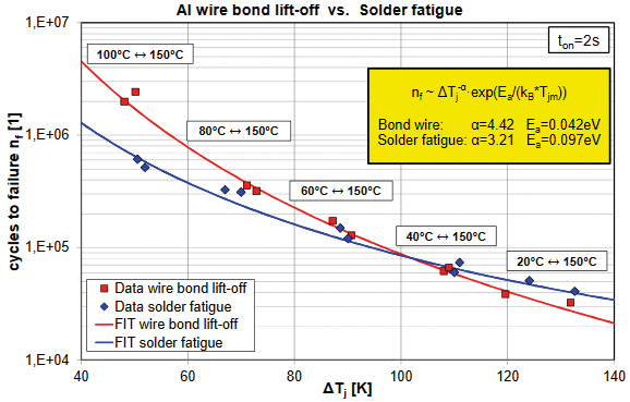 Fig. 24: Influence of deltaTjmax and Tm on solder fatigue and Al wire bond degradation [122]The progress in the development of lifetime models for the interpretation of life cycle limitations of power modules under thermo-mechanical stress shows that the complete documentation of the test conditions and the power modules considered is essential for the development and comparison of power cycling results.
The methodology of power cycling is described in [120, 123, 124], but especially in [121] and [122, 125]. Figure 24 shows the influence of deltaTjmax and the temperature Tm, here as an example for solder joints and Al wire bonds. Figure 25 shows the results of Cu sintering in comparison with Pb-containing solders in the number of cycles to EOL (end of live). The figure shows the achievable number of defect-free cycles in comparison with Pb-containing solders and the Cu sintered bond.
In addition to Figure 25, [53] describes more than 1 million power cycles at a temperature difference of DTj =110K until the DCB interface to the sintered joint broke, leading to an increase in thermal resistance and ultimately to defects [53]. In [114, 125], the combination of power cycling with the FEM method is discussed in order to compare the prediction with the experimental results.
|
Substrate technology |
Insulating dielectric material |
Metalization |
Coating of the metallization |
Optional dendritic growth and time for different fluids |
||||
|
Tap water |
Deionized water |
Di water with H2SO4 |
Di water with HCI |
|||||
|
1 |
DBC |
AIN |
Cu |
- |
Yes |
Yes |
Yes |
Yes |
|
2 |
DBC |
Al2O3 |
Cu |
- |
Yes |
Yes |
Yes |
Yes |
|
3 |
DBC |
Cu |
Ag |
Yes |
Yes |
Yes |
Yes |
|
|
4 |
DBC |
Al2O3 |
Cu |
Ag |
Yes |
Yes |
Yes |
Yes |
|
5 |
DBC |
Cu |
Au |
No |
No |
Yes |
No |
|
|
6 |
AlSi soldered |
Al2O3 |
Al |
Ni |
No |
No |
No, but surface corrosion |
No, but surface corrosion |
|
7 |
IMS |
Al2O3 filled epoxy |
Cu |
Ag |
Yes |
Yes |
Yes |
Yes |
|
8 |
DBA direct casting |
AlN |
Al |
Ni |
No, but surface corrosion |
No, but surface corrosion |
No, but surface corrosion |
No, but surface corrosion |
|
9 |
AMB CuAgTi solder |
Si3N4 |
Cu |
Ni |
No, but surface corrosion |
No |
Yes |
Yes |
Tab. 4: Power electronics module carriers [DCB, IMS, DBA, AMB) and corrosion results after exposure to different fluids [105]
H3TRB test
In [73], the H3TRB test is compared with the THB [temperature, humidity, bias]. The advantage of the H3TRB test compared to the THB test is the use of higher voltages. Both tests promote charges or ion movement, support the detection of instabilities depending on process variation or faulty design variants. However, by applying higher voltages in the H3TRB test, corrosion mechanisms are accelerated by electrochemical mechanisms, which play a dominant role under field conditions compared to the classical effects of charges or ion movement.
 Fig. 25: Number of defect-free cycles comparing Pb solder and Cu sintering technology [125]. Reliability limited by wire bonding and the connection of the upper electrode
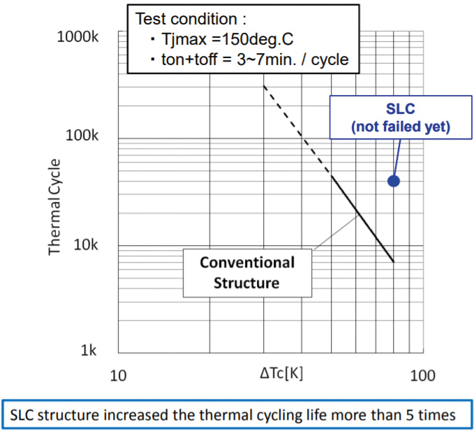 Fig. 26: Thermal cycles as a function of delta Tc [127]
Under conditions of high electric fields and sufficient humidity, ions react on the chip surface, which can cause electrochemical corrosion. Furthermore, the use of high test voltages provides more realistic lifetime estimates. The test voltage is in the range of later operating conditions. In [50], the H3TRB test is used to estimate the service life for 30 years.
Encapsulation
Mold compounds [36] with Tg greater than 174 °C are presented. In [109], resin-based epoxy systems with Tg between 180 and 210 °C and CTE values of 16 ppm/K are presented, which are used in particular in harsh environments. [127] reports on mold compounds with Tg greater than Tj at CTE values of 16 ppm/K and high adhesion strength (SLC). Figure 26 shows the dependence of the defect-free number of power cycles on the delta Tc. Low temperatures of -70°C are achieved without significant degradation, as the resin base does not exhibit any criticalization effects [127]. The warpage is approximately negligible.
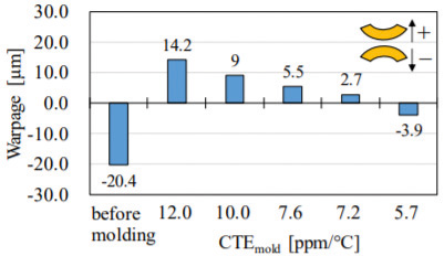 Fig. 27: Results module warpage depending on the CTE value [86][86] describes mold compounds with higher Tg and adjusted CTE values(Fig. 24) in order to achieve high reliability values [114]. Figure 27 shows the dependence of the warpage on the CTE value of the developed mold compound. A low warpage level is conducive to guaranteeing stable interfaces between chip substrate and mold compound module and keeping the resistance approximately stable.
The further development of ceramic coating materials and technologies is described in [128, 129](Fig. 28). The focus is on adjusting the CTE values to minimize the mechanical stress in the overall composite.
In [129] molding materials are described as solutions for GaN power devices. In addition to the CTE adjustment to the CTE values of the WBG materials, the high thermal stability, the high thermal conductivity and the high corrosion resistance are emphasized.
FEM for Power Electronics
FEM modeling is used, among other things, to compare the experimental results of the power cycle test with the material and design dependency module structures [57, 82, 85, 107, 114, 117, 119, 125]. Furthermore, the FEM results are used to estimate elastic and plastic deformations in the joining part plane, in particular in the area of the die attach. In [131], the void formation is simulated as a function of the process parameters. The dependence of the temperature distribution in Ag-sintered Cu substrates on the sintering pressure is determined in [132].
 Fig. 28: Schematic structure of a conventional power module with TMC (Thermal Mass Circuit) [128]
The new failure mechanisms occur depending on the mechanical material characteristics such as the modulus of elasticity, the CTE value and the geometry of all components in the module assembly. Furthermore, the usual deformations of the die and the substrates can be determined, which are essential for a reliable lateral bond. The warpage results in particular are part of the thermally dependent stabilities/instabilities in the module composite.
 Fig. 29: Out-of-plane deformation of a sintered IGBT at 25 °C and 250 °C [84]Figure 29 shows the warpage results of an IGBT at RT and at 250 °C. The transition from convex to concave deformation is striking, which firstly leads the die attach to interface instabilities at higher temperatures and secondly poses a risk of breakage of the semiconductor. The energy densities, which are determined during the FE analysis, are used to estimate the fracture toughness as a fracture indicator in the materials and the interfaces.
Tests Sinter Interconnects
Part 1 lists the internationally applied temperature cycling tests. Temperature cycling, e.g. between -40/+250 °C, demonstrates the importance of developing functional materials.
Industry Standard Tests-Reliability
Standards for reliability tests are not yet available, but are urgently needed in order to be able to compare the results of passive (temperature cycle test) and active (power cycle test) cycle tests. A proposal for standardization was presented in [130] and is used to thermally characterize the Rth value in the module assembly(Fig. 30). An SIC microheater chip was developed.
The proposed measurement conditions define the reliability, reproducibility and have a high resolution. The proposed method has a standard deviation of 0.01K/W.
 Fig. 30: Experimental configuration for determining the Rth value [130]
Summary
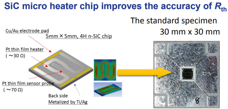 Fig. 31: SiC microheater improves the accuracy of the Rth value [130] The two-part article 'Sintering Technology - An Overview' attempts to review the technological features of sintering technology from the perspective of the literature in order to capture and describe the trend of the applicative features. The range of influencing factors and variables to ensure the highest possible reliability of high-temperature-suitable joints becomes visible. In addition to Ag sintering technology, Cu sintering technology is described as being equivalent in terms of application and, in the case of Cu sintering technology, also guarantees a precious metal-free joining process.
Literature
[1] Hutzler, A.: Improvement of Power Module Systems Solders by Directional Solidification, CIPS, 2018
[2] Albrecht; Busse; Dahlbüdding: Sintering Technology - An Overview, Part 1, PLUS Magazine, 2020
[3] De Monchy: New Sintering Form Factors for Next Generation Power Modules, ECPE, 2019
[4] von Ribbeck: Laserbonding: The perfect connection, ECPE, 2019
[5] Schmitt: Pressureless sintering of large dies by infrared radiation, CIPS, 2018
[6] Guo-Quan Lu: Advanced Die-attach by Metal-powder Sintering: The Science and Practice, CIPS, 2018
[7] Hinrich: Reliability of Sintered Die Top Systems in Power Cycling Tests, ECPE, 2019
[8] Nakako: Sintered Cu bonding pastes and their bonding reliabilities, ECPE, 2019
[9] Feißt: Power Chip Interconnections Based on TLP and Sintering of CTE-Matched Conductors, CIPS, 2018
[10] Steenmann: TLPB Improves Solder Connections by On Chip Creation of Intermetallic Phase Precursors, EMPC, 2019
[11] Aasmundtveit: High-energy X-ray Tomography for 3D Void Characterization in Au[Sn Solid-Liquid Interdiffusion (SLID) Bonds, EMPC, 2019
[12] Huebner, S.; Penka, B.; Barchmann, M.; Eigner, W.; Gruber, M.; Nobis, et al.: Microcontacts with sub-30 µm pitch for 3D chip-on-chip integration, Microelectronic Engineering, vol. 83, Nov-Dec 2006, 2155-2162
[13] Luu, T.T.; Duan, A.; Aasmundtveit, K.E.; Hoivik, N.: Optimized Cu-Sn waferlevel bonding using intermetallic phase characterization, Journal of Electronic Materials, vol. 42, 2013, 3582-3592
[14] Honrao, C.; Huang, T.C.; Kobayashi, M.; Smet, V.; Raj, P.M.; Tummala, R.: Accelerated SLID bonding using thin multi-layer copper-solder stack for finepitch interconnections, in 2014 IEEE 64th Electronic Components and Technology Conference (ECTC), 2014, 1160-1165
[15] Tollefsen, T.A.; Larsson, A.; Lovvik, O.M.; Aasmundtveit, K.: Au-Sn SLID Bonding-Properties and Possibilities, Metallurgical and Materials Transactions B-Process Metallurgy and Materials Processing Science, vol. 43, Apr 2012, 397-405
[16] Johnson, R.; Wang, C.Q.; Liu, Y.; Scofield, J.D.: Power Device Packaging Technologies for Extreme Environments, IEEE Transactions on Electronics Packaging Manufacturing, vol. 30, 2007, 182-193
[17] Rautiainen, A.; Xu, H.B.; Osterlund, E.; Li, J.; Vuorinen, V.; Paulasto-Krockel, M.: Microstructural Characterization and Mechanical Performance of Wafer-Level SLID Bonded Au-Sn and Cu-Sn Seal Rings for MEMS Encapsulation, Journal of Electronic Materials, vol. 44, pp. Nov 2015, 4533- 4548
[18] Aasmundtveit,K.E.; Luu, T.T.; Nguyen, H.-V.; Larsson, A.; Tollefsen, T.A.: Intermetallic Bonding for HighTemperature Microelectronics and Microsystems: Solid-Liquid Interdiffusion Bonding, in Intermetallic Compounds - Formation and Applications, M. Aliofkhazraei, Ed, ed Open Access: Intech Open, 2018
[19] Status of the Power Electronics Industry 2015 reporting on power eletronics market by IHS Yole Développement, www.IHS.com
[20] [3] Charbonnier J. et al.: 3D integration for power MOS H bridge power application, Chip Scale Review, Vol. 20, No. 4 (2016), 30-33
[21] Charbonnier J. et al.: Silicon 3D integration for small power devices, in Electronic SystemIntegration Technology Conference (ESTC), 2016 IEEE 6th, Grenoble, 13-15 Sept. 2016
[22] Rudzki: Evolution of Sinter Paste, ECPE, 2019
[23] Streibel: Reliability of SiC MOSFET with Danfoss Bond Buffer Technology in Automotive Traction Power Modules, PCIM, 2019
[24] Miric: Heraeus and the challenge of new packaging solution for power modules, ECPE Workshop, 2019
[25] Abibe: Danfoss Silicon Power Novel Die Top Connections using Cu Wires and Ribbons, ECPE, 2019
[26] Scheuermann: Basic Interconnections, ECPE Workshop, 2019
[27] Guth: New packaging technologies for power electronic modules, ECPE Workshop, 2029
[28] Kuziora: Bi Behavior in Au-(In-Bi) SLID Bonding, ESTC, 2020
[29] Ko; Chen: Low temperature bonding technology for 3D integration, Microelectron. Reliab, vol. 52, no. 2, 2012, 302- 311
[30] Charbonnier: Towards Wafer Level 3D Power Integration, CIPS, 2018
[31] Welker: On the Thermal Performance of Si3N4-Based Ceramic Multilayer Substrates, PCIM, 2019
[32] Yasui: A 3.3 kV 1000 A High Power Density SiC Power Module with Sintered Copper Die Attach Technology, PCIM, 2019
[33] Polezhaev Development of a novel 600V[50A power package with semiconductor chips sandwiched between PCB substrates using double-side Ag-sintering, PCIM, 2019
[34] Ostmann: Power modules with embedded components," European Microelectronics and Packaging Conference, EMPC, 2013
[35] Kearney: PCB embedded power electronics for low volt-age applications, International Conference on Integrated Power Systems, CIPS, 2016
[36] Otto: Investigating the mold compounds influence on power cycling lifetime of discrete power devices, PCIM, 2019
[37] Hinrich: Failure Mechanisms of Sintered Die Top Systems under Power Cycling Tests, PCIM, 2019
[38] Streibel: Reliability of SiC MOSFET with Danfoss Bond Buffer Technology in Automotive Traction Power Modules, PCIM, 2019
[39] Becker: FEM based enhancement of system lifetime by improvement of the die top connection of power electronic semiconductors, Nuremberg, CIPS, 2018
[40] Nakako: Relationship Between Bonding Properties and Porosity of Sintered Cu Bonding, PCIM, 2019
[41] Dechant: Performance of a GaN Half Bridge Switching Cell with Substrate Integrated Chips, PCIM, 2019
[42] Yamauchi: The characteristics of Sintered Copper Layer by Pressure Sintering Process for Power Module Application, PCIM, 2019
[43] Müller: Selective Silver Sintering on Organic-Based Circuit Boards, PCIM, 2019
[44] Watanabe: Stable Microstructure and Mechanical Properties of Pressureless Sintered Silver at a Temperature of 250 ºC, PCIM, 2019
[45] Takata: Sintering Cu Paste on Cu Plates with Different Metallization, PCIM, 2019
[46] Gao: Highly Reliable Package using Cu Particles Sinter Paste for Next Generation Power Devices, PCIM, 2019
[47] Mohn: Reliable interconnection technologies for high-temperature operation of SiC MOSFETs, PCIM, 2017
[48] Nakako: Sintering Copper Die-Bonding Paste Curable Under Pressureless Conditions, PCIM, 2017
[49] Miyazaki: Development of thermal fatigue-tolerant active metal brazing substrates using highly-thermal conductive silicon nitrides with high toughness, PCIM, 2017
[50] Kitajima: Lifetime estimation model of HVIGBT considering humidity, PCIM, 2017
[51] Favre: A double side cooled Electronic Power Module, PCIM, 2017
[52] Zhou: A Novel SiC Power Module with 3D Integration, PCIM, 2017
[53] Schmidt: Power Cycle Testing of Sintered SiC-MOSFETs, PCIM, 2017
[54] Watanabe: Material Design and Process Conditions of Pressureless Sintered Silver for 200/-40 ºC Thermal Cycling Reliability, PCIM, 2017
[55] Zacharias: Performance Comparison of fast Silicon and Silicon Carbide Devices used with conventional PCBs and embedded into PCBs, PCIM, 2017
[56] Hinze: Aufbau- und Verbindungstechnik für PV-Wechselrichter, Master Thesis, University of Kassel, 2013
[57] Varley: Thermo-Mechanical Optimization of Press-Pack IGBT Packaging Using Finite Element Method Simulation, PCIM, 2017
[58] Bicakzi: Thermo-Mechanical Optimization of Press-Pack IGBT Packaging Using Finite Element Method Simulation, ECPE Workshop, 2019
[59] Bartsch; LTCC as substrate - enabling semiconductor and packaging integration, EMPC, 2019
[60] Sebastian: Low loss dielectric matarials for LTCC applications: A review, International Materials Review, Vol. 53, 2013
[61] Inoue: Design of Interfacial Chemistry for Inducing Low Temperature Sintering of Silver Micro-fillers within Epoxy-based Binders, EMPC, 2019
[62] Aasmundtveit: High-energy X-ray Tomography for 3D Void Characterization in AucSn Solid-Liquid Interdiffusion (SLID) Bonds, EMPC, 2019
[63] Bhogaraju: Hybrid Cu particel paste with surface modified particles for high temperature packaging, EMPC, 2019
[64] Stenzel: Characterization of alternative sinter materials fot power electronics, EMPC, 2019
[65] Nishikawa: Effect of bonding temperature on shear strength of joints using micro-sized Ag particles for high temperature packaging technology, EMPC, 2019
[66] Reinhardt: PrintPOWER - Paste systems for multifunctional copper power modules, EMPC, 2019
[67] Gökdeniz: Behavior of Silver-Sintered Joints by Cyclic Mechanical Loading and Influence of Temperature, EMPC, 2019
[68] Liu: High temperature wireless packaging of SiC power device by organic-free die-attach material sintering, PCIM, 2019
[69] Schwarzer: Investigation of pressureless sintered interconnections on plasma based additive copper metallization foe 3-dimensional ceramic substrates in high temperature applications, ECPM, 2019
[70] Herman: Plasma-Sprayed Coatings, Scientific American, vol. 259, no. 3, 1988, 112u117, JSTOR
[71] Hensel: Investigations of Silver Sintered Interconnections 3- Dimensional Ceramics with Plasma Based Additive Copper Metallizations, 20th IEEE Electronics Packaging Technology Conference, EPTC, 4.12.2018
[72] Wargulski: Paving the way for the replacement of solder interconnections in power electronics by silver-sinter using pulsed infrared thermography, ECPM, 2019
[73] Kolbinger: An approach for failure prediction in H3TRB-tests, ECPM, 2019
[74] Damian: Low Temperature Wafer Bonding Based on Copper Nanoparticle Sintering for 3D Interconnect Fabrication, CICT, 2020
[75] Scheuermann: Limitation of Power Module Lifetime Derived from Active Power Cycling Tests, CIPS, 2018
[76] Müter: Simulation of the Thermal Transient Behavior of Silicon Carbide Modules Using Liquid Convection Cooling, CIPS, 2018
[77] Bayer: Interpretation of Power Cycling Data derived from transient Cooling Curves, CIPS, 2018
[78] Rittner: Innovative Reliable Nitride based Power Devices and Applications - The EU Public Funded Project InRel-NPower, CIPS, 2018
[79] Reiner: PCB-Embedding for GaN-on-Si Power Devices and ICs, CIPS, 2018
[80] Göbl: Direct Pressed Die (DPD) Technology - a Novel Packaging Solution for Power Modules, CIPS, 2018
[81] Schnur: Design and Fabrication of PCB Embedded Power Module with Integrated Heat Exchanger for Dielectric Coolant, CIPS, 2018
[82] Becker: FEM based enhancement of system lifetime by improvement of the die top connection of power electronic semiconductors, CIPS, 2018
[83] Charbonnier: Towards Wafer Level 3D Power Integration, CIPS, 2018
[84] Naumann: Thermo-mechanical stress and deformation behavior of joined semiconductor devices using different die attach technologies, CIPS, 2018
[85] Dudek: Combined experimental- and FEstudies on sinter-Ag behavior and effects on IGBTmodule reliability, 15th International Conference on Thermal, Mechanical and Mulit-Physics Simulation and Experiments in Microelectronics and Microsystems (EuroSimE), Ghent, 2014, 1-9, doi: 10.1109[EuroSimE.2014.6813870
[86] Mitamura: A transfer-molded high temperature SiC power module withstanding up to 250 °C, CIPS, 2018
[87] Makiire: Thermal Characteristic Evaluation and Transient Thermal Analysis of Next-generation SiC Power Module at 250 °C, CIPS, 2018
[88] Takemasa: Die-bonding performance of micron Ag particle paste for high power devices, CIPS, 2018
[89] Abe: Dielectric Properties and Partial Discharge Inception Voltage of Aluminum Nitride Insulating Substrate at High Temperatures, CIPS, 2018
[90] Mitamura: A transfer-molded high temperature SiC power module withstanding up to 250 °C, CIPS, 2018
[91] Kim : GaN micro-heater chip for power cycling of die attach modules with Ag sinter joint and high temperature solder, PCIM, 2019
[92] Aschenbrenner: Heterogeneous Integration to Enable Future Smart Systems, ESTC, 2020
[93] Klein: Power module design for utilizing of WBG switching performance, PCIM, 2019
[94] Göbl: Direct Pressed Die (DPD) Technology - a Novel Packaging Solution for Power Modules, CIPS, 2018#
[95] Stoll: Additive Manufacturing for Power Electronics Substrate Technologies, ECPE, 2019
[96] Schnur: Design and Fabrication of PCB Embedded Power Module with Integrated Heat Exchanger for Dielectric Coolant, CIPS, 2018
[97] Schweizer Electronic: 60 % Performance Increase by Power Mosfet Embedding, ECPE, 2019
[98] Polezhaev: Development of a novel 600V/50A power package with semiconductor chips sandwiched between PCB substrates using double-side Ag-sintering, PCIM, 2019
[99] Dechant: Performance of a GaN Half Bridge Switching Cell with Substrate Integrated Chips, PCIM, 2019
[100] Müller : Selective Silver Sintering on Organic-Based Circuit Boards, PCIM, 2019
[101] Scheuermann: Limitation of Power Module Lifetime Derived from Active Power Cycling Tests, CIPS, 2018
[102] Mouawad: On the reliability of stacked metallized ceramic substrates under thermal cycling, CIPS, 2018
[103] Miyazakia: Effect of high temperature cycling on both crack formation in ceramics and delamination of copper layers in silicon nitride active metal brazing substrates, Ceram. Int, vol. 43, 2017, 5080-5088
[104] Bach: Vias in DBC Substrates for Embedded Power Modules, CIPS, 2018
[105] Bayer: Electrochemical Corrosion on Ceramic Substrates for PowerElectronics - Causes, Phenomenological Description, and Outlook, CIPS, 2018
[106] Bayer: LTCC Embedding of SiC Power Devices for High Temperature Applications over 400 °C, ESTC, 2020
[107] Dudek: FE Analyses and Power Cycling Tests on the Thermo-Mechanical Performance of Silver Sintered Power Semiconductors with Different Interconnection Technologies, ITherm, 2017
[108] Satoh: Cu-Zn Alloy Bonding Using Cu Nanoparticles and Zn Powder for Packaging of Semiconductore Power Devices, Mate, 2020
[109] Kaji: Development of Encapsulation Technology of Epoxy Resin for High Temperature operating Power Modules, Mate, 2020
[110] Welker: On the Thermal Performance of Si3N4-Based Ceramic Multilayer Substrates, PCIM, 2019
[111] Yasui: A 3.3 kV 1000 A High Power Density SiC Power Module with Sintered Copper Die Attach Technology, PCIM, 2019
[112] Polezhaev: Development of a novel 600V[50A power package with semiconductor chips sandwiched between PCB substrates using double-side Ag-sintering, PCIM, 2019
[113] Otto,.: Investigating the mold compounds influence on power cycling lifetime of discrete power devices, PCIM, 2019
[114] Hinrich: Failure Mechanisms of Sintered Die Top Systems under Power Cycling Tests, PCIM, 2019
[115] Junghaenel: Investigation on Isolated Failure Mechanisms in Active Power Cycle Testing, PCIM, 2015
[116] Ruzki: Power Modules with Increased Power Density and Reliability Using Cu Wire Bonds on Sintered Metal Buffer Layers, CIPS, 2014
[117] Dudek: Combined experimental- and FEstudies on sinter-Ag behavior and effects on IGBT-module reliability, EuroSimE ,2014
[118] Naumann: Thermo-mechanical stress and deformation behavior of joined semiconductor devices using different die attach technologies, CIPS, 2018
[119] Becker: FEM based enhancement of system lifetime by improvement of the die top connection of power electronic semiconductors, CIPS, 2018
[120] Dai: Power cycling reliability of time-reduced sintering for attaching SiC diodes using nanosilver film, CIPS, 2018
[121] Luo: [115] Dai: Power cycling reliability of time-reduced sintering for attaching SiC diodes using nanosilver film, CIPS 2018
[122] Scheuermann: Limitation of Power Module Lifetime Derived from Active Power Cycling Tests, CIPS, 2018
[123] Hinrich: Reliability of Sintered Die Top Systems in Power Cycling Tests, ECPE, 2019
[124] Kim: GaN micro-heater chip for power cycling of die attach modules with Ag sinter joint and high temperature solder, PCIM, 2019
[125] Lutz: Power Cycling of Packages with SiC Devices, ECPE Workshop, 13.1.2020
[126] Welker: Power System in Package based on Multilayer Ceramic Substates, ECPE Workshop, 9.10.2019
[127] Idaka: New developments in resin encapsulated power module, ECPE Workshop, 10.10.2019
[128] Behrendt: New thermal designs of power modules with inorganic encapsulation, ECPE Workshop, 10.10.2019
[129] Yu: Ceramic embedding as packaging solution for future power electronic application, ECPE Workshop, 10.10.2019
[130] Wakasugi: Thermal property evaluation of next-generation power modules, ESTC, 2020
[131] Carisey: Low temperature fine pitch vertical wafer level interconnection using copper nanoparticles, CITC, 2020
[132] Zhang: Investigation of Pressure Assisted Nanosilver Sintering Process for Application in PowerElectronics, CITC, 2020
