Würth Elektronik CBT has been working on the development of stretchable and moldable circuits - also known as stretchable and conformable electronics - for several years. In 2016, a technology for manufacturing stretchable electronic systems based on conventional PCB production processes was completed. This technology has been available in series production as TWINflex-Stretch since 2018. Instead of rigid glass fiber-reinforced epoxy resin-based materials or flexible polyimide films, stretchable polyurethane substrates are used and straight conductor paths are replaced by meandering conductors. These innovative electronic systems combine properties such as flexibility, elasticity, malleability and flexibility. As a result, these circuit carriers can adapt flexibly to free-form surfaces and are ideal for integration into textiles and wearables as well as 3D surfaces. The soft and skin-friendly properties of polyurethanes are predestined for use in medical applications. In various projects with customers from the medical, sensor and automotive technology sectors, various stretchable polyurethane-based printed circuit boards have been produced. Textile-integrated bandages and lighting systems, stretchable FPC (Stretchable PCB), electrode arrangements for EMG are just a few examples. Part 2 of this technical article will appear in PLUS 7/2020.
Würth Elektronik CBT has been working on the development of stretchable and formable circuits - also known as stretchable and conformable electronics - for several years. In 2016, a technology for the production of stretchable electronic systems based on conventional processes of printed circuit board manufacturing was completed. Since 2018 this technology is available in series as TWINflex-Stretch. Instead of rigid glass fiber reinforced epoxy resin based materials or flexible polyimide foils, stretchable substrates made of polyurethane are used and straight conductors are replaced by meander-shaped conductors. These new types of electronic systems combine properties such as flexibility, elasticity, formability and bending slackness. Therefore, these circuit carriers can be flexibly adapted to free-form surfaces and are ideal for integration in textiles and wearables as well as for 3D surfaces. The soft and skin-friendly properties of the polyurethanes are predestined for use in medical applications. Various stretchable polyurethane-based printed circuit boards have been produced in various projects with customers from the medical, sensor and automotive industries. Textile-integrated bandages and light systems, stretchable FPC (Stretchable PCB), electrode arrangements for EMG are some examples. Part 2 of this article is published in PLUS 7/2020.
Flexible electronic circuits have been used in many products for several decades and are now state of the art. The continuing trend towards miniaturization with increasing functionalization means that ever smaller installation spaces in all three dimensions are to be used in a space-saving manner by bending, rolling or folding(Fig. 1).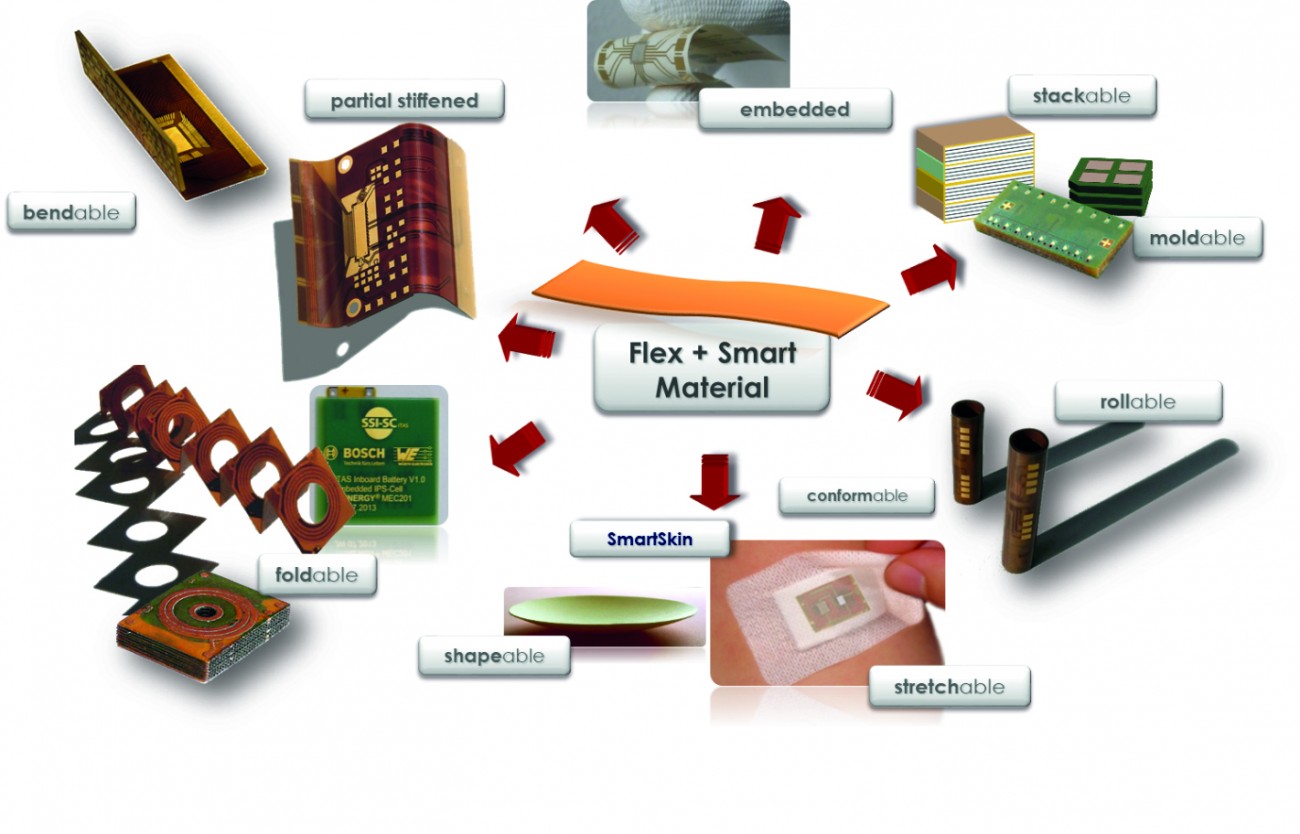 Fig. 1: System in foil variants
With the help of technologies established in the printed circuit board industry such as flex-rigid, but also through further processing by folding or rolling flexible printed circuit boards, many geometric structures can be captured, but the deformation is usually limited to one axis.
Electronic systems that can retain their electrical functionality during three-dimensional mechanical deformation create new possibilities such as the ability to adapt to surfaces of any shape or to cope with reversible stretching and are therefore recommended for many areas such as medical technology or prosthetics, soft robotics, wearables or textiles.
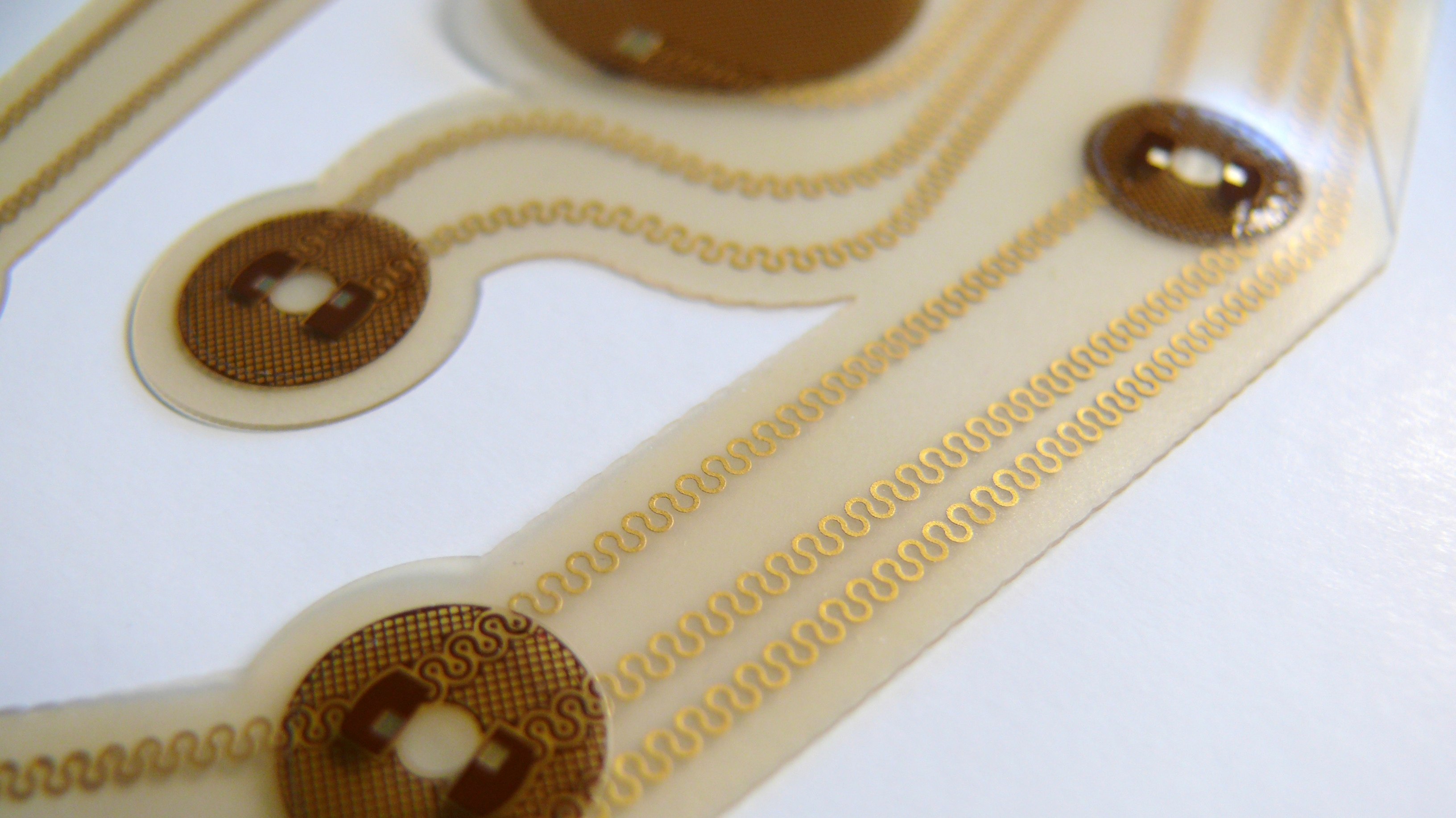
New constructions based on polyurethane or silicone materials, nonwovens and textiles, but also stretchable conductors made of metal or polymer and thin or printed electronic components are therefore the focus of many research projects. Stretchable polyurethane printed circuit boards offer a simpler and practical implementation(Fig. 2).  Fig. 2: TWINflex-Stretch - Stretchable polyurethane-based printed circuit board A significant advantage: The circuit carriers introduced to the market as TWINflex-Stretch are realized using adapted but conventional wet-chemical etching techniques, whereby the stretchability of the metallic conductors can be achieved by a special meander design [1, 2].
Stretchable substrates based on thermoplastic polyurethane
Thermoplastic polyurethane is produced from diols and isocyanates without the use of plasticizers and is available in various forms, from hard to soft to elastic. Due to its broad property profile, this polymer has a wide range of applications. In everyday life, we often encounter polyurethane in a foamed state. Products such as mattresses, shoe soles or imitation leather are made from this raw material. The multiblock co-polymer consists of 'hard' and 'soft' segments. This allows properties such as flexibility, elasticity and stretchability to be realized. They are ideal for use in textiles or wearables.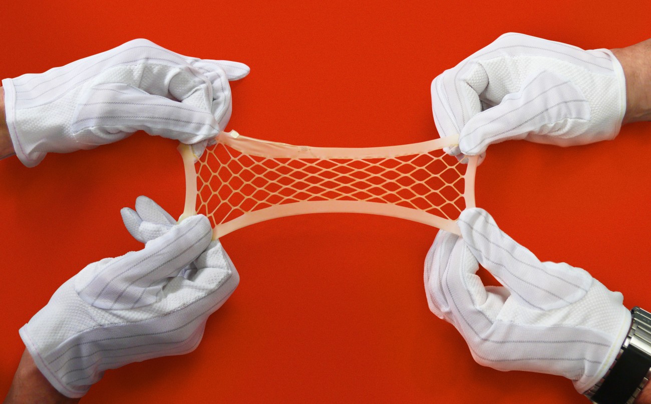 Fig. 3: Stretchable polyurethane printed circuit boards
The high surface energy makes polyurethane scratch and wear resistant. Polyurethane is also known to have characteristic properties such as high tear resistance and good thermal insulation properties. This is why this material is often used as a surface coating for furniture or fittings, as a thermal barrier or, when mixed with fillers, to increase the stability of building structures.
In the electronics industry, this material is used at most as a base for adhesives or potting compounds. Thermoplastic polyurethane films as a carrier material in the printed circuit board industry are a novelty.
The hydrolysis and microbe resistance as well as the physical bonding of all additives in the polymer matrix enable skin-friendly and biocompatible applications. This paves the way for the use of these substrates in the medical sector.
Typical printed circuit board processing of stretchable substrates / industrial production
Polyurethane adheres excellently to copper and has good physical and chemical stability, so that it can also be used as a base material in printed circuit board technology. Polyurethane is available for printed circuit boards in thicknesses of 50 to 200 µm and can be processed safely at temperatures <140 °C.
The thin transparent films were not originally developed for the PCB industry. New paths had to be taken here too. The advantage is the use of processes typical for printed circuit boards. The required laminates are produced in a first production step by laminating with copper foils. The adhesive strength is 2 to 4 times higher compared to polyimide (PI) or FR4. Conventional wet-chemical structuring and etching processes are then used.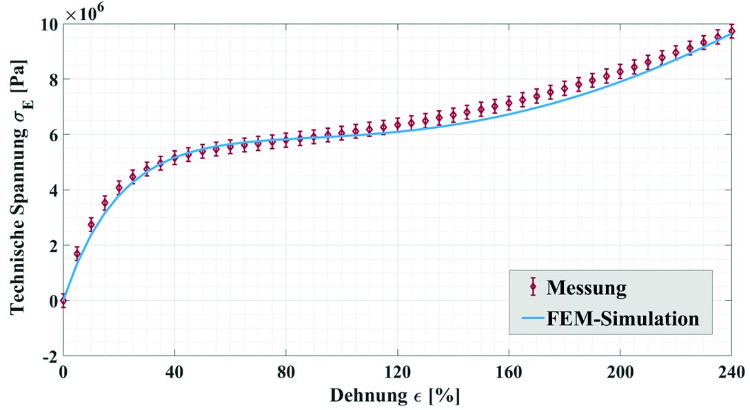 Fig. 4: TWINflex-Stretch stretchable printed circuit boards
Würth Elektronik was the first company to succeed in manufacturing the highly elastic polyurethane film under series production conditions as a sample and also in larger quantities. The typical production format for samples is 18 x 12". The advantages of these construction variants are easy to recognize:
- Almost any shape can be realized with a flexible and adaptable material
- Dynamic elongation of up to 20% is possible
- The layout design and component selection does not have to change, as standard PCB structures and dimensions are maintained
- Typical layout designs and conventional surface finishing allow SMD assembly, but low-temperature solders must be used here
- Further processing options such as bonding, welding, lamination, overmoulding or forming allow these circuit carriers to be used in many different applications
 Fig. 6: Relative change in resistance taking into account the circuit track geometry (double logarithmic plot)

Properties of stretchable substrates
As with rigid and flexible substrate materials, there is a wide range of options for the choice of material and structure. Factors such as biocompatibility, the maximum stretchability required in the end application, processing compatibility, adhesion between metal and substrate and breathability are decisive. Depending on the application, the limits must be measured and defined. The mechanical properties of the final circuit are essentially influenced by the copper layout. Since copper, like all metals, has a low intrinsic ductility, the conductor path structures must be formed into a suitable two-dimensional meander geometry. This special design can significantly influence the ductility of the metallic conductors. Depending on the 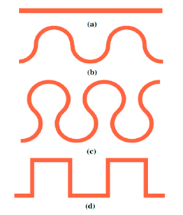 Fig. 5: Stress-strain relationship of the measurement data and FEM simulation of TPU conductor track geometry, an expansion of between 5 and 20 % can be achieved for dynamic applications. A one-off expansion of up to 60 % can also be reliably achieved.
When designing the meander geometry, countless variations are initially conceivable. For this reason, it is difficult to determine the basic technology parameters for a desired expansion. This makes it all the more important to find an optimum geometry in the interplay between the achievable properties and manufacturability. Parameters such as the change in meander design, conductor width and spacing as well as height influence the expandability of the overall system. Furthermore, issues such as solder stop, cover foil and subsequent assembly should not be neglected.
In order to guarantee controllable properties, in-depth knowledge of the materials used and layout limits is essential. For this reason, the characterization and multiphysical modelling of stretchable thermoplastic polyurethane and meandering copper conductor paths are required. Due to the large number of parameters, the quantitative investigation of stretchability proved to be a very difficult task. In a first test, the influence of the meander structure on the ductility was investigated. For this purpose, various conductor track geometries were subjected to a dynamic load and the number of elongation cycles was determined. Due to their plastic properties, straight copper conductor paths cannot withstand high tensile stresses or deformations adequately and can lead to material failure and thus to a loss of function of the circuit carrier. The meander conductor tracks, on the other hand, could be reversibly stretched up to 10,000 times depending on the layout. Unexpectedly, the rectangular structures showed the best performance. An increase in the number of cycles can be expected through further and targeted optimization of the conductor path geometry. These results could be confirmed with the help of finite element simulation (FEM) using COMSOL Multiphysics, which shows good agreement between measurement and simulation [11].
Compared to conventional printed circuit board technologies, stretchable polyurethane substrates are more flexible due to their high degree of flexibility and good biological Fig. 7: Stress curves when optimizing the angular geometry:
(a) angular geometry 1.0 % elongation
(b) angular geometry 5.0 % elongation
(c) Radius 60 µm at 1.0 % elongation
(d) Radius 60 µm at 5.0 % elongation
(e) Radius 100 µm at 1.0 % elongation
(f) Radius 100 µm at 5.0 % elongation Compatibility as a future technology in the field of medical applications has great potential. Using innovative, additive technologies to produce functional layers on an elastic polyurethane matrix and embedding passive or active components in conjunction with the development of shaping processes, a significant expansion of the range of functions can be achieved while at the same time reducing the amount of space required. In order to compensate for the volume change during thermal forming processes without impairing the electrical conductivity, the conductor paths must be designed as meander structures.
A hyperelastic material model by Mooney [17] and Rivlin [18] was used to characterize the stress-strain behaviour of polyurethane under high strain.
This allowed parameters such as material constants, compression modulus and transverse contraction to be extracted. The values of the extracted parameters were used to create a finite element simulation (FEM) using COMSOL Multiphysics [11]. This simulation finally produced the stress-strain curves illustrated in Figure 5. A good agreement between measurement and simulation can be observed.
In addition to the hyperelastic material models, the embedded conductor path structures are also of particular importance. When implementing copper traces in TPU, their antagonistic behavior with regard to the stress-strain characteristics, the change in resistance during the stretching process (and the associated electrical conductivity) and the mechanical stresses that occur must be taken into account.
The investigation of different conductor geometries is an important step towards the optimum conductor geometry. On the basis of FEM simulations, optimization potentials are identified with regard to the targeted adaptation of geometries to reduce stress peaks during deformation.
|
Geometry |
norm. Initial resistance |
von Mises voltage |
von Mises voltage |
|
even |
100 % |
100 % |
100 % |
|
180° meander |
157 % |
90 % |
122 % |
|
270° meander |
333 % |
26 % |
76 % |
|
angular |
291 % |
26 % |
100 % |
Four different structures were
compared with each other:
a) straight conductor paths,
b) meandering geometry with a series of 180° arcs (semicircles),
c) meandering geometry with a series of 270° arcs (horseshoe),
d) meandering geometry with angular structures
Meander construction
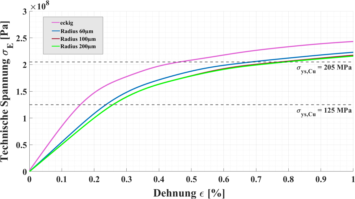 Fig. 8: Stress-strain curve as a function of radius sizeRectilinearcopper conductor paths cannot withstand high tensile stresses or deformations due to their plastic properties and can lead to material failure and thus to a loss of function of the circuit carrier. On the basis of an FEM model, basic statements can be made regarding conductivity and the associated relative change in resistance even at strain rates of 5 %. As the double logarithmic plot in Figure 6 shows, 270° meanders and angular track structures appear to be particularly suitable for the purpose of deformation, while straight track geometries show high resistance changes in comparison and are therefore no longer considered in further analyses.
The occurring stress values are of primary interest. In addition to the normalized initial resistance R0,norm., the average von Mises voltage σM,aver. and the maximum values of the von Mises voltage σM,max. are also used for the evaluation. Although the normalized initial resistance R0,norm appears comparatively high both for a 270° meander and for the angular structure, this can be attributed to the length allowance due to the geometric conditions (see Table 1).
This example shows that the mechanical stresses can be reduced by up to 74 % by selecting suitable conductor track structures. This means that the stretchable circuit carrier can withstand significantly more pronounced tensile stresses or deformations before potential material failure occurs.
As is known from the field of technical mechanics, stress peaks occur more frequently at corners and edges of components. Therefore, in Figure 7, different sized radii were integrated into the angular track geometry from Figure 6 in order to analyze the effects on the stress curve. Starting from a track width of 100 µm, radii of 60 µm, 100 µm and 200 µm were implemented.
The results of the FEM simulations with regard to the resulting stress curves for the square original variant and a conductor track with a radius of 60 µm and 100 µm are shown as examples. Figures a), c) and e) show the occurring von Mises stresses at a strain of 1 %. Figures b), d) and f) represent stress states at 5 % elongation. The color legend can be used as an indicator of the stress maxima for interpretation. The original geometry already shows clear stresses at 1 % elongation, which already show critical values with increasing elongation up to 5 % and which can indicate material fatigue. When integrating a radius of 100 µm, on the other hand, the stress values already drop by approx. 10 %.
Specific material characteristics relating to the plasticity model of Cu are also used as a basis for evaluation. Plasticity effects are subject to elasto-plastic material models. A characteristic criterion is an ideal elastic behavior of the material as long as a certain stress limit is undercut. Two parameters are defined for the transition area between elastic behavior and the beginning of flow of such a material, which are considered critical limit values - the initial yield stress for the analyzed Cu (is 125 MPa) and the actual yield stress (205 MPa). If all the parameters and characteristics presented are visualized in a logical manner, statements on the optimization potential of conductor geometries can be derived from this causal relationship and on the basis of Figure 8.
Literature:
[1] J. Kostelnik: Flexible and Stretchable PCBs for Smart Electronics - TWINflex-Concept; Visions to Products - MID and Beyond, Stuttgart, DOI: 10.13140/RG.2.2.16785.48485, 10.10.2017
[2] A. Schreivogel; J. Kostelnik: More than flexible - Stretchable Electronic Solutions, BE-FLEXIBLE, Munich, 11.2016
[3] T. Someya: Stretchable Electronics, Wiley VCH, 2013
[4] ULTIMUM - UltraThin flexible Microsystems - BMBF project (16SV5136); https://www.pronto-ultimum.de
[5] KoSiF - Complex systems in foil - BMBF project (16ES00016); http://kosif.ims-chips.de
[6] J. Kostelnik: Die funktionelle Integration von aktiven und passiven Komponenten in die Leiterplatte im industriellen Umfeld, Systemintegration in der Mikroelektronik: Embedding-Technologien und ihre Wertschöpfungskette bei elektronischen Baugruppen; Congress, Nuremberg June 8-10, 2010, SMT Hybrid Packaging, Ed.: H. Reichl, VDE Verlag GmbH, Berlin/Offenbach
[7] S. Saller; C. Harendt; J. Kostelnik; A. Schreivogel; Y. Mahsereci; J. Burghartz: SmartSkin - An intelligent skin for adaptive bionic grippers, Mikrosystemtechnik Kongress 2015, Karlsruhe, October 26-28, 2015
[8] K.F. Becker et al.: Embedding technologies for an automotive radar system, 2009, 59th Electronic Components and Technology Conference, San Diego, CA, 2009, 1453-1459, DOI: 10.1109/ECTC.2009.5074203
[9] A. Kugler; M. Koyuncu; A. Zimmermann; J. Kostelnik: Chip Embedding in Laminates, 159-165, In: Ultra-thin Chip Technology and Applications, Springer, New York, NY, DOI 10.1007/978-1-4419-7276-7_14
[10] http://intakt-projekt.de/
[11] N. Philippin; A. Schreivogel; I. Kühne; J. Kostelnik: Electronics of a new dimension - Potentials of stretchable film systems in the development of interactive microimplants, EBL 2020, Fellbach
[12] C. Kallmayer; F. Schaller; T. Löher; J. Haberland, F. Kayatz; A. Schult: Optimized Thermoforming Process for Conformable Electronics, In: 2018 13th International Congress Molded Interconnect Devices (MID) IEEE (2018), pp. 1-6
[13] https://applause-ecsel.eu/
[14] K.-P. Hoffmann et al: Technical, Medical and Ethical Challenges in Networks of Smart Active Implants, 41st Annual Intern. Conference IEEE EMBC (2019), pp. 1484-1487
[15] K. Birkner: SnBiAg1 in der Serienfertigung (SnBiAg1 for serial production), DVS-Berichte 273, Symposium on Soft Soldering - Research & Practice for Electronics Production, Hanau, 2011
[16] M. Nowottnick; A. Novikov; J. Trodler: Possibilities and Limits of Bismuth Solders, P.195-200, SMTA International, Rosemont, IL, USA, Sep. 17-21, 2017
[17] M. Mooney: A Theory of Large Elastic Deformation. Journal of Appl. Physics, 11 (1940) H.9, pp. 582-592
[18] R. Rivlin: Large elastic deformations of isotropic materials. I. Fundamental concepts, Philosophical Transactions of the Royal Society of London, Series A.: Mathematical and Physical Sciences, 240 (1948) H.822, pp. 459-49
[19] P. Schwarzmann: Thermoforming: A practical guide, 2nd ed. Hanser Publications, 2019
