Würth Elektronik CBT has been working on the development of stretchable and moldable circuits - also known as stretchable and conformable electronics - for several years. In 2016, a technology for manufacturing stretchable electronic systems based on conventional PCB production processes was completed. This technology has been available in series production as TWINflex-Stretch since 2018. Various stretchable polyurethane-based printed circuit boards have been produced in various projects with customers from the medical, sensor and automotive technology sectors. Textile-integrated bandages and lighting systems, stretchable FPC (Stretchable PCB), electrode arrangements for EMG are just a few examples. Part 1 of this technical article appeared in PLUS 6/2020.
Würth Elektronik CBT has been working on the development of stretchable and formable circuits - also known as stretchable and conformable electronics - for several years. In 2016, a technology for the production of stretchable electronic systems based on conventional processes of printed circuit board manufacturing was completed. Since 2018 this technology is available in series as TWINflex-Stretch. Various stretchable polyurethane-based printed circuit boards have been produced in various projects with customers from the medical, sensor and automotive industries. Textile-integrated bandages and light systems, stretchable FPC (Stretchable PCB), electrode arrangements for EMG are some examples. Part 1 of this article appeared in PLUS 6/2020. ") Fig. 8: Stress-strain curve as a function of radius size (repetition of part 1)
Fig. 8: Stress-strain curve as a function of radius size (repetition of part 1)
As can be seen from Figure 8, the application of radii within the angular track geometry leads to a significantly improved stress-strain behavior. The optimization has a significant effect on the strain properties for radius sizes of 100 µm and 200 µm. The yield point is also reached with a significant delay and higher tensile stresses are possible. With regard to the development of circuit carriers for medical implants, an angular track geometry with embedded radii is therefore recommended.
To validate the data and findings obtained through FEM simulations, a measurement setup was implemented as shown in Figure 9, with which systematic measurements of the stress-strain characteristics of the circuit carriers can be carried out.
The results obtained support the previous statements. Figure 10 demonstrates the result of a measurement with an elongation of the TWINflex stretch circuit carrier of up to approx. 60 %. A plot of the relative resistance changes against the strain and a comparison with the FEM simulation shows that the generated simulation models reliably represent the stress-strain relationship as well as the behavior of the resistance change of such a TPU-Cu composite.
Resistance change curve for measurement and simulation
If a circuit carrier of this type is subjected to a higher strain than 55 %, the copper conductor track will crack. Furthermore, delamination occurs between TPU and Cu, which can be seen in Figure 11.
In summary, it can be stated that TPU is predestined for use in medical technology. The investigations have shown that TPU can be described by the Mooney-Rivlin material model. It was also demonstrated that the optimization of conductor geometries can significantly improve the elongation characteristics.
Due to the low softening temperature of polyurethane, the stretch PCBs are assembled in a low-temperature reflow process. A solder based on tin/bismuth (Sn/Bi), which is processed at approx. 140 °C (melting temperature: 138 °C), can be used here (Fig. 12). Initial estimates show that the use of tin-bismuth solder has two significant advantages over conventional lead-free SAC solders.
 Fig. 9: Measurement setup for expandable circuit carriers
 Fig. 10: Resistance change curve for measurement and simulation
 Originalzustand des Schaltungsträgers; b) Riss des Cu-Mäanders sowie Delamination zwischen TPU und Cu durch starke Dehnungsbeanspruchung") Fig. 11: a) Original condition of the circuit carrier; b) Crack in the Cu meander and delamination between TPU and Cu due to strong tensile stress
Fig. 11: a) Original condition of the circuit carrier; b) Crack in the Cu meander and delamination between TPU and Cu due to strong tensile stress
 Fig. 12: Polyurethane circuit board fitted with Sn/Bi solder
 Fig. 13: Demonstrator of a thermally formed TWINflex consisting of LCP film and foamed HTT-PEI carrier
 Fig. 14: Demonstrator of a 3D thermoformed HTT carrier made of PEI foam
 Fig. 15: Demonstrator of an assembled and subsequently back-molded polyimide film
The main advantages of SnBi solder are [15,16]:
- less stress on the assembly during soldering
- Lower energy consumption of up to 30% (this also means lower CO2 emissions)
Application examples for 3D electronics based on thermoplastics
In various research and customer projects, such as HTT-Board and Drusym, initial possibilities and uses for thermal forming (Fig. 13, 14) and for targeted, functional back-molding or overmolding of film materials (Fig. 15) have already been demonstrated.
Interesting fields of application for these technologies can be found above all in the automotive and medical sectors. In the field of medicine, the design of medical implants for the treatment of complex medical conditions is one of the most important key technologies of our time. The INTAKT innovation cluster [10], initiated by the German Federal Ministry of Education and Research (BMBF), is focusing on the development and preclinical testing of interactive microimplants in this context. Among other things, innovative therapeutic approaches are to be realized in the form of stretchable and flexible catheters for the suppression of widespread tinnitus, which can be implanted in the cochlea for the purpose of electrical stimulation [14]. The aspect of material and immaterial biocompatibility of all materials used must always be taken into account [11]. Furthermore, the individual adaptability of implants to the respective body contour is of great importance in order to ensure adequate wearing comfort. As already described in 2.4, the transfer of electronic components into the third dimension allows, for example, the embedding of passive or active components and significantly expands the range of functions while simultaneously reducing the space required. This type of free-formability and behavior like a second, intelligent skin (SmartSkin) or organic surface (soft, adaptable) is virtually predestined for medical technology applications and ensures excellent accuracy of fit. In the future, this approach with polyurethane (TPU) may also offer interesting approaches for catheters, for example, compared to the currently more frequently used thermoplastic liquid crystal polymer (LCP).
 Fig. 16: Logitech demonstrator - back-injected polyurethane film
 Fig. 17: SmartSkin I demonstrator in LCP
 – CHIP+ Technologie") Fig. 18: SmartSkin I demonstrator in LCP (Liqud Crystal Polymer) - CHIP+ technology
Fig. 18: SmartSkin I demonstrator in LCP (Liqud Crystal Polymer) - CHIP+ technology
SmartSkin - LCP
With SmartSkin I, a first application demonstrator for an intelligent skin was presented in the joint funding project KoSiF [5]. Here, four ultra-thin chips were integrated into a flexible substrate and attached to the adaptive bionic Finray gripper [7] (Fig. 17: Demonstrator with LCP substrate). The basic prerequisite is a suitable embedding technology (CHIP+) for embedding thin chips in films, which was already developed in the previous Ultimum project [4, 6, 9]. The main difference to standard embedded chips, as described in KRAFAS [8], is that the entire structure including the chip retains sufficient flexibility (Fig. 18) and can therefore be used for a wide range of applications in the wearable, healthcare and soft robotics sectors.
SmartSkin II - EMG electrodes
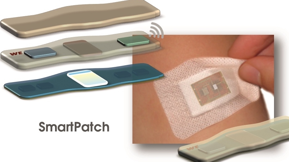
As a new substrate for PCB production, polyurethane is providing a boost to innovation in electronics. The technology has now been transferred from the development stage to series production  Fig. 19: TWINflex-Stretch electrode array for EMG applications. Single-sided and double-sided PCBs as well as flexible systems with partial reinforcement are offered under the name TWINflex-Stretch. The first customer projects have been implemented. The focus is not always on electrical performance, but properties such as stretchability or softness are the decisive arguments for customers. Furthermore, further processing technologies are also an important factor, as the new printed circuit boards can be bonded, welded, formed, etc. Due to this wide range of properties, stretchable TWINflex-Stretch printed circuit boards have many applications in the fields of medical technology, sensor technology, automotive, wearable or smart textiles and soft robotics as so-called stretchable electronics [3].
With suitable end surfaces, skin-friendly or even biocompatible PCBs can be realized for medical technology. Figure 19 shows an example of an electrode array for the electrical stimulation of muscles.
This functional sensor structure based on polyurethane, realized using PCB technology, has several electrode elements with a silver surface and can be used in the rehabilitation of paralyzed muscles, for example in stroke patients. Stimulation takes place via individual elements or via several elements. This means that several muscle groups can be addressed. The flexibility of PI and LCP foils is not sufficient for this application. In contrast, the particularly soft, flexible and skin-friendly PU fits very well and comfortably to the irregular shape of the forearm and leaves fewer marks on the skin. Similar applications directly on the skin or embedded in a textile can be realized with this technology.
 Fig. 20: Manufacturing process of the planar TWINflex stretch circuit carrier as an upstream step to thermoforming, SHAPEflex
SmartSkin III - Neonatology
The TWINflex-Stretch concept has already been transferred to series production. In an application from the Swiss company SenTecAG, a stretchable circuit board from Würth Elektronik is integrated into a measuring belt that is applied to the skin. The belt allows the lung function of infants to be measured very gently and carefully without intervention and observed by the doctor in dynamic images. The use of radiology is no longer necessary.
These belts are based on the principle of electrical impedance tomography. Electrical impedance tomography (EIT) is an imaging technique for intensive care physicians, pulmonologists and physiotherapists that provides real-time information on regional ventilation. In contrast to conventional methods, no ionizing X-rays are used and EIT can be applied over several days. EIT can therefore be used continuously and to monitor treatment effectiveness in real time directly at the patient's bedside. There are currently no comparable devices that can display such regional organ function continuously and in real time at the patient's bedside.
SHAPEflex - further development based on polyurethane substrates
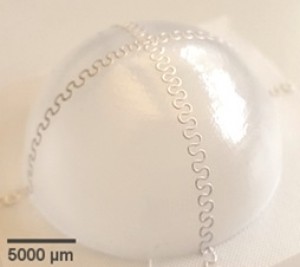
Stretchable circuit carriers open up even more geometric design and miniaturization options. On the one hand, the polyurethane-based PCB can be further processed in established assembly processes. On the other hand, many new design options are available to achieve the desired shape or functionality. For example, assembled or unassembled stretch films can be laminated, soldered, glued or welded to various substrates such as textiles, polymers or metals. Polyurethane develops its adhesive properties at elevated temperatures. This enables very good adhesion to be achieved on many substrates. For some time now, circuit carriers such as the TWINflex-Stretch variant have been given a completely new meaning by their transfer to the third dimension. This technology, known as 'conformable electronics', is revolutionizing the field of application-specific electronics in many areas and, in this context, is also gradually finding its way into medical technology [12]. The INTAKT innovation cluster [10] uses this technological approach to develop circuit carriers for their location in interactive microimplants. A rudimentary prototype with an integrated lens for optical communication can be seen in Figure 21. The intention behind this additional placement of the circuit carrier lies in the possibility of significantly increasing the scope of integration and functionality by equipping the circuit carrier with active or passive components. This should also enable, for example, the embedding of antennas or coils for the realization of an inductive energy supply. As an upstream step to the thermoforming process, the previously planar TWINflex stretch circuit carrier is produced using established PCB manufacturing processes. A composite of thermoplastic polyurethane and polycarbonate has proven itself as a material combination for thermoplastic shaping. Both materials have similar softening temperatures. Together with the embedding of copper conductor tracks in meander form, the materials enter into a symbiosis during plastic forming.


Fig. 21: 3D-printed implant housing with embedded lens for optical communication and SHAPEflex circuit carrier placed in the base element of the housing
 entformtes Substrat (b) Schaltungsträger nach Entfernung des überschüssigen Materials")
 entformtes Substrat (b) Schaltungsträger nach Entfernung des überschüssigen Materials")
Fig. 22: SHAPEflex circuit carrier after thermoforming: (a) demolded substrate (b) circuit carrier after removal of excess material
The underlying process of thermoforming, also synonymous with the term deep drawing, has long since crossed the threshold to market entry in some production areas and can therefore also be seen as a pioneer for applications in the segment of innovative circuit carrier technologies. This technology has manifested itself, for example, in the automotive industry for the molding of interior components or in the packaging industry. Thermoforming is the forming of thermoplastic materials under high heat. In terms of functionality and the cost-efficient production of molded parts, five main process steps have become established over time [19]: 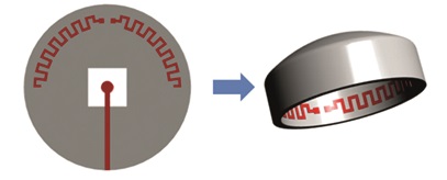
- Heating of a planar semi-finished product
up to the softening temperature - Pre-stretching of the substrate
- Molding of the positive or negative geometry
of the target structure - Defined cooling of the mold produced
to room temperature - Demolding of the three-dimensional workpiece

An example of a demoulded circuit carrier is visualized in Figure 22. Low-temperature solder pastes with a melting point below the softening temperature of TPU and PC are used for the subsequent assembly of the now three-dimensional SHAPEflex circuit carriers in order to avoid material damage. There are therefore virtually no limits to the individual shaping of three-dimensional circuit carriers. The processability of the materials prior to forming using conventional production methods also makes this technology very interesting from an economic point of view.
According to this concept, circuit carriers can be transformed from 2D into a 3D shape after assembly. Flat printed functions (e.g. antenna) but also discrete components could be accommodated directly in the housing or cover in this way. This type of free-formability (SHAPEflex) is virtually predestined for medical technology applications and guarantees excellent accuracy of fit. This technology could, for example, complement the existing 3D-MID technology and is particularly suitable for large-area and lightweight electronics [1].
Summary and outlook
With TWINflex-Stretch, STRETCHflex and SHAPEflex, a new and innovative solution for 3D electronics is available for various areas of application. With this development, a new type of PCB technology has been implemented and established on the market, which could lead to expansion and even change in the electronics market Fig. 23: Multifunctional hybrid integration - combination of 3D electronics with stretchable silver conductive pastes on an integrated stretch PCB - SHAPEflex. The advantages of a conventional printed circuit board (stability, multiple layers, assembly, etc.) and new properties of flexible polyurethane films (stretchability, softness, biocompatibility) are combined in the new 'rigid-stretchable' technology.
Intelligent, networked implants are becoming increasingly important in solving complex medical problems. Under the coordination of the Fraunhofer Institute for Biomedical Engineering IBMT, new generations of active, networked implants are being developed in the publicly funded INTAKT project. Nerve and muscle structures are to be stimulated on the basis of medical measurements recorded in real time and controlled by the patient. The development focus of these innovative, adaptive systems is on the design of completely new human-technology interactions between patients and their implants as well as the treating physician. The project aims to generate a basic technology that is as universal as possible for a wide range of medical applications. These include the suppression of tinnitus, the partial restoration of gripping functions of the hand and the treatment of gastrointestinal motility disorders. Stretchable polyurethanes are an innovative variant that can be used for dynamic applications (muscle and tissue movements) as TWINflex-Stretch circuit carriers in extracorporeal systems. As SHAPEflex, the polyurethane/polycarbonate composite can serve directly as part of the overall construction of the implant and thus offers various possibilities for integrating different functions.
Work is also currently underway in European research projects such as APPLAUSE [13] on the development of electronic patches.
Literature:
[1] J. Kostelnik: Flexible and Stretchable PCBs for Smart Electronics - TWINflex-Concept; Visions to Products - MID and Beyond, Stuttgart, DOI: 10.13140/RG.2.2.16785.48485; 10.10.2017
[ 2] A. Schreivogel; J. Kostelnik: More than flexible - Stretchable Electronic Solutions, BE-FLEXIBLE, Munich, 11.2016 [ 3] T. Someya: Stretchable Electronics, Wiley VCH, 2013
[4] ULTIMUM - UltraThin flexible Microsystems - BMBF project (16SV5136), https://www.pronto-ultimum.de
[5] KoSiF - Complex systems in foil - BMBF project (16ES00016), http://kosif.ims-chips.de
[6] J. Kostelnik: Die funktionelle Integration von aktiven und passiven Komponenten in die Leiterplatte im industriellen Umfeld, Systemintegration in der Mikroelektronik: Embedding-Technologien und ihre Wertschöpfungskette bei elektronischen Baugruppen, Congress, Nuremberg June 8-10, 2010, SMT Hybrid Packaging, Ed.: H. Reichl, VDE Verlag GmbH, Berlin/Offenbach
[7] S. Saller; C. Harendt; J. Kostelnik; A. Schreivogel; Y. Mahsereci; J. Burghartz: SmartSkin - An intelligent skin for adaptive bionic grippers, Mikrosystemtechnik Kongress 2015, Karlsruhe, October 26-28, 2015
[8] K.F. Becker et al.: Embedding technologies for an automotive radar system, 59th Electronic Components and Technology Conference, San Diego, CA, 2009, 1453-1459, DOI: 10.1109/ECTC.2009.5074203
[9] A. Kugler; M. Koyuncu; A. Zimmermann; J. Kostelnik: Chip Embedding in Laminates, 159-165, In: Ultra-thin Chip Technology and Applications, Springer, New York, NY, DOI 10.1007/978-1-4419-7276-7_14
[10 ] http://intakt-projekt.de/
[11 ] N. Philippin; A. Schreivogel; I. Kühne; J. Kostelnik: Electronics of a new dimension - Potentials of stretchable film systems in the development of interactive microimplants, EBL 2020, Fellbach
[12] C. Kallmayer; F. Schaller; T. Löher; J. Haberland; F. Kayatz; A. Schult: Optimized Thermoforming Process for Conformable Electronics, In: 13th International Congress Molded Interconnect Devices (MID) IEEE, 2018, 1-6
[13] https://applause-ecsel.eu/
[14] K.-P. Hoffmann et al: Technical, Medical and Ethical Challenges in Networks of Smart Active Implants, 41st Annual Intern. Conference IEEE EMBC, 2019, 1484-1487
[15] K. Birkner: SnBiAg1 in der Serienfertigung (SnBiAg1 for serial production), DVS-Berichte 273, Symposium on Soft Soldering - Research & Practice for Electronics Production, Hanau, 2011
[16] M. Nowottnick; A. Novikov; J. Trodler: Possibilities and Limits of Bismuth Solders, P.195-200, SMTA International, Rosemont, IL, USA, Sep. 17-21, 2017
[17] M. Mooney: A Theory of Large Elastic Deformation. Journal of Appl. Physics, 11, H. 9, 1940, 582-592
[18] R. Rivlin: Large elastic deformations of isotropic materials, I. Fundamental concepts, Philosophical Transactions of the Royal Society of London, Series A.: Mathematical and Physical Sciences, 240,H. 822, 1948, 459-49
[19] P. Schwarzmann: Thermoforming: A practical guide, 2nd ed. Hanser Publications, 2019
