
Building on IAVT developments for the ZIM-funded PowerBoard project, the LogiPow concept was created, which implements highly reliable wiring solutions for power and logic electronics on the basis of organic printed circuit boards. An application demonstrator from the automotive sector has already been successfully implemented.
Based on IAVT developments for the ZIM-funded project PowerBoard, the concept LogiPow was developed, which realizes wiring solutions of power and logic electronics on the basis of organic printed circuit boards in a highly reliable way. An application demonstrator from the automotive sector could already be successfully implemented.
Motivation
For power electronic applications, e.g. electrified and electric drive technology, commercially used drones, e-charging stations or any energy conversion systems, electronic assemblies are required which, in addition to a fundamentally high degree of miniaturization, also offer high energy efficiency and a spatially and technically tight integration of power components (switches, inductors, capacitors, etc.) and logic components (microcontrollers, signal processors, modules for wireless communication, memory, etc.).
Electromobility in particular demands solutions from electronics developers that are suitable for high switching currents and power densities and at the same time have a high packing density and low weight. Solutions for control electronics for mobile machinery, on-board power supply components for 48 V and high-voltage electrical systems and drive inverters in electric vehicles, among others, place high demands on packaging and connection technology. There is an increasing demand for the integration of power and logic electronics for regulating and controlling switching currents and digital network technology within a single electronic assembly. In addition to assembly technologies based on ceramic wiring carriers, those based on organic printed circuit boards are entering the market, as they offer cost advantages and allow flexible adaptation to the installation space.
![]()

Fig. 1: Structural concept for printed circuit boards based on LogiPow technology (left) and technology demonstrator (right)
Technological concept
For the development of such solutions, a concept for organic PCBs with a thick structured copper core layer for power transmission and simultaneous heat dissipation combined with a localized multilayer insert for the logic electronics was initially designed(Fig. 1). The concept follows current market requirements for solutions for power electronic assemblies in the power range >20 kW and builds on the developments that were developed at the Institute of Packaging Technology at the Technical University of Dresden as part of the ZIM-funded PowerBoard project [1]. Due to the integration of power and logic electronic wiring solutions, the concept is called LogiPow. In addition to the miniaturization of the logic electronics and thus short cable lengths and a high wiring density, this concept also allows good heat dissipation of the power electronics while simultaneously reducing weight. Following extensive technological part developments for the manufacture and integration of the individual PCB components, an application demonstrator from the automotive sector was successfully implemented.
 Fig. 2: Classification of LogiPow technology based on the continuous current carrying capacity and maximum number of layers for the logic part
LogiPow technology: Classification in the market environment
The innovative LogiPow technology is another form of technology alongside the existing PCB technologies. The traditional technologies of IMS (Insulated Metal Layer), metal core technology (according to IPC600) and multi-layer thick copper technology have their advantages in terms of heat dissipation and carrying capacity of high electrical currents. Specific and partially protected technologies, such as Wirelaid, Power Combi, Smart p²-Pack, Iceberg or HSMtec each bring functionalities to the printed circuit board and combine them to form functional hybrid solutions. LogiPow technology differs technologically from these solutions and shows its potential in the fact that electrical currents of up to 600 A can be conducted and dissipated within a PCB and the logic electronics can be integrated on the same circuit carrier with multilayer technology of up to 14 layers(Fig. 2). The technology fulfills the following requirements:
- high packing density with logic and power structures
- low weight for mobile applications
- high continuous current carrying capacity
- high number of layers in the logic area and
- high heat dissipation capacity with
- design with reduced installation space.
LogiPow technology also meets the process requirements for integration into the standard PCB manufacturing process, giving it a cost advantage over other combination technologies.
The technology in detail
The innovative production of the new technology is characterized by the fact that it is as close as possible to the standard PCB process. First, a stable bond between laminates, prepregs and one or more copper inserts is produced using a pressing process(Fig. 3). The result is a laminate or semi-finished product with inserts that are sealed on both sides. This is where LogiPow technology clearly sets itself apart from previous solutions. The resulting semi-finished product is of high quality in terms of its mechanical stability and freedom from cavities. This is achieved by the prepreg resin penetrating from the inside to the outside and filling the cavities between the laminates and the inserts. The resulting semi-finished product can then be further processed like conventional laminates in the standard PCB process. Not only is it possible to structure the outer laminate sides, but it is also possible to galvanically bond the outer layers to the inserts.
 Fig. 3: Schematic representation of the production process for a LogiPow PCB
Currently implemented LogiPow assemblies contain copper inserts with a thickness of 2 mm, although this is not a limitation. In order to be able to implement this copper thickness in thick copper technology, 4 layers with a thickness of 400 µm and 2 layers with a thickness of 200 µm would have to be arranged.
In order to achieve electrical properties equivalent to the new concept presented here, these 6 layers would have to be connected by additional holes. This results in an additional electroplating process and additional plugging to close these holes again before the next pressing process. Compared to the LogiPow variant, the thick copper layers do not allow the same structurability in terms of line/space. In the newly introduced technology, these structures can be arranged within the laminates (L2-L5) due to the lower copper thickness. With thick copper technology, additional copper layers are required for this. For these reasons, the number of layers in thick copper technology increases from 6 to 10 levels.
In addition, a different technological process must be used for structuring copper thicknesses of 200 or 400 µm, as the resist used as standard, which is also used for LogiPow, cannot withstand the etching of copper of this thickness. For thick copper technology, a metal resist associated with additional process steps is required.
Even after the first pressing operation, it is clear that the PCB thicknesses differ significantly due to the high number of thick copper layers and the need to press them: The thickness of the LogiPow structure is 2.0 mm, that of the thick copper variant 4.5 mm.
The additional multilayer structure enables all design options in the PCB process, as no cavities need to be filled between laminates and inserts. Likewise, no additional resin depots need to be considered for filling. This means that a small gap can be created between the LogiPow semi-finished product and the outer layers. This has a positive effect on heat dissipation.
In a production comparison between thick copper technology and the technology presented, advantages in terms of PCB thickness, weight, structurability, material price and manufacturing costs were demonstrated(Table 1).
The production process makes it possible to integrate different materials. Not only metal cores (copper, aluminum, ...), ceramics or metal composite materials (such as aluminum roll-clad with copper) can be integrated, but also laminates can be produced, which enable selective hybrid structures with locally integrated, e.g. high-frequency-capable organic substrates. Even the integration of glass is conceivable with this process. Material cost savings can be generated for such products and new material combinations with a wide range of properties can be provided, opening up new application possibilities.
The technology therefore clearly stands out from previously known processes in terms of its manufacturing technology, manufacturability, variability and the expansion of possible applications.
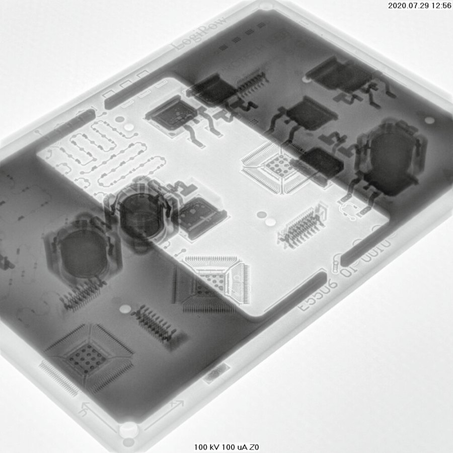

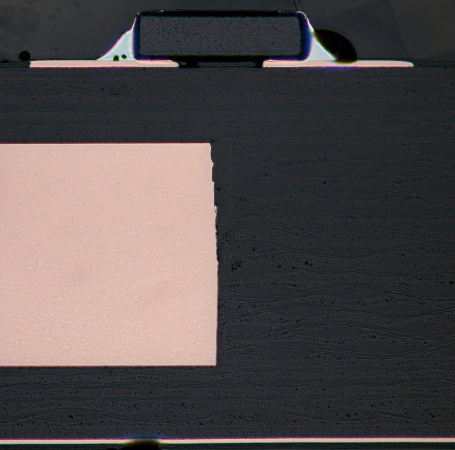
Fig. 4: Radiography (left) and micrograph (right) of LogiPow test carriers show the position of the integrated copper inserts and the successful assembly of various components (including CC/CR, DPAK, QFP, LGA), as well as the layer structure consisting of a copper insert in the inner layer, standard copper in the two outer layers and high-Tg-FR4
As part of the project, various test substrates were designed and finally manufactured at industrial level. Figure 4 shows representative examples of the technological implementation. The radiography(Fig. 4 left) clearly shows the expansion and arrangement of the copper inserts in a test carrier for investigating the thermo-mechanical reliability of a LogiPow PCB. The radiography also shows the mixed assembly of the PCB. On the right of the image, a metallographic section shows the layer structure used for this test carrier. The flawless joining of the copper insert in accordance with the technology (see also Fig. 3), the delamination-free layer structure on the top and bottom of the semi-finished product and the soldering of LGA and CR components, for example, in accordance with the specifications are clearly visible. The proven high production quality is a basic building block for fulfilling the functional and thermo-mechanical requirements of a LogiPow PCB. The microanalytical approach effectively supported the rapid development of the technology.
Material and interface investigations

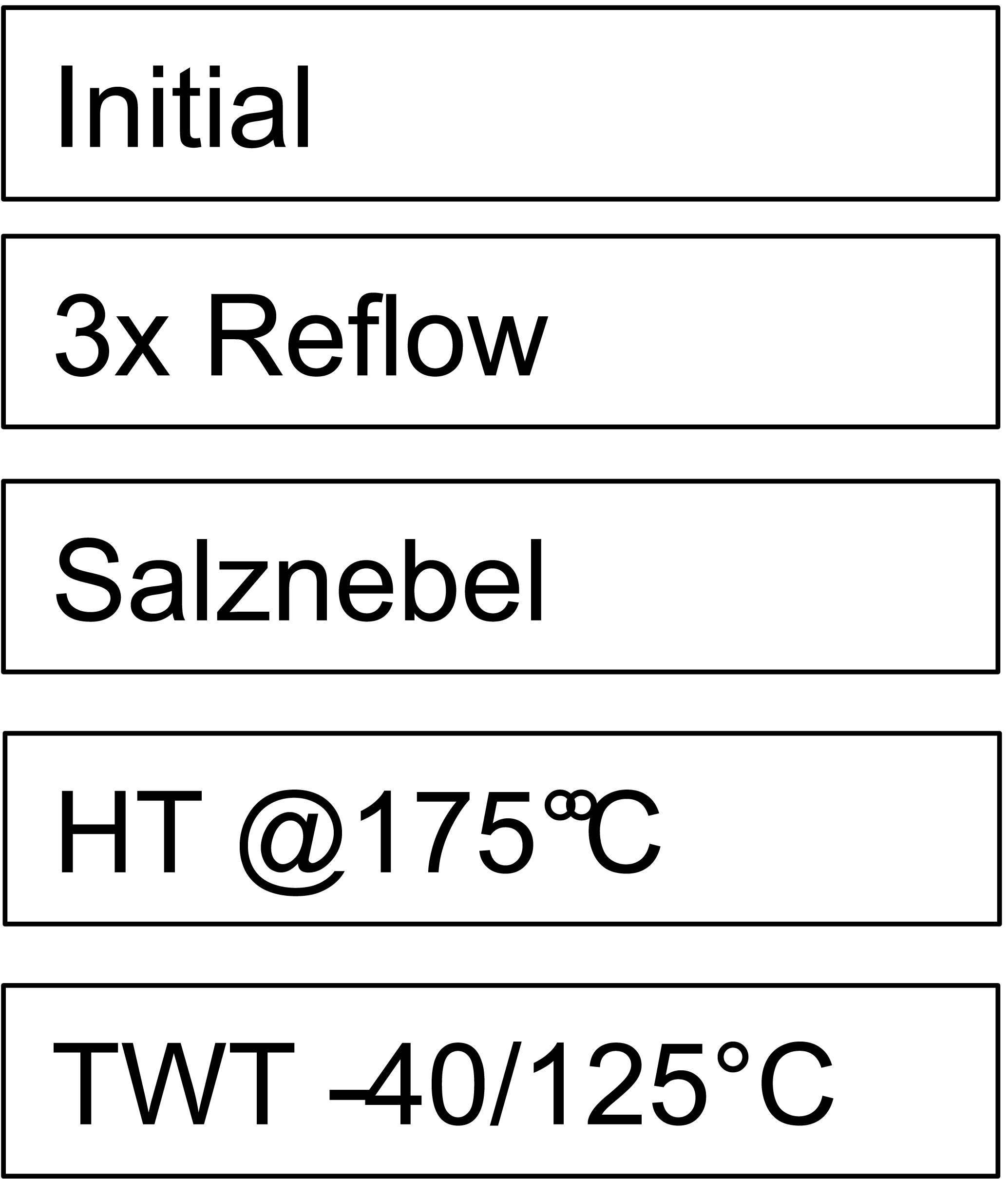 Fig. 5: Overview of the strip samples before and after aging shows externally recognizable degradation effectsTheadhesion and interface properties of the resin to copper material play a decisive role in the overall reliability. The degradation behavior and mechanical stability were tested on strip test specimens made of 2 mm thick copper with a 2-4 mm polymer-filled insulation gap(Fig. 5). The focus was on the adhesion at the interfaces and the cohesion of the polymer material (370HR resin) under external environmental loads. Four environmental tests were carried out on the rod-shaped mechanical test specimens: triple reflow soldering, salt spray test according to DIN EN ISO 9227, high-temperature exposure at 175 °C and an automotive-oriented temperature cycling test (-40 °C/+125 °C 30'/30'). Figure 5 shows test specimens before and after the various environmental tests and shows their ageing due to thermal degradation or corrosion.
A mechanical 4-point bending test was used to determine the bending stiffness and breaking strength before and after the environmental test. These tests were carried out at 20 °C and 150 °C in order to take temperature dependencies into account. A strain rate-controlled test sequence with a speed of 0.1 µm/s was selected. The mechanical characteristic values and the fracture behavior were recorded at the beginning and during the course of the environmental tests. The measured variable system stiffness [GPa] indicates the elastic behavior of the entire test specimen or the material composite. The flexural strength indicates the maximum mechanical stress [MPa] that the test specimen can withstand.
As expected,Figure 6 shows a lower flexural strength at 150 °C than at room temperature (20 °C). This is due to the lower storage modulus of the resin at 150 °C. No fractures or defects were detected. The 3-fold reflow soldering process shows no significant influence. The polymer is already sufficiently cross-linked in the initial state and post-cross-linking does not take place. After high-temperature aging as well as after the temperature cycling test, a slight approx. 10 % reduction in system stiffness was observed.
 Fig. 6: Comparison of initial state with various ageing states of the bending mode system stiffness at 20 °C and 150 °C
Figure 7 shows the measured breaking strengths before and after the environmental tests. The 3-fold reflow has a minor influence on the strength (approx. -15 %). This is also reflected in the predominantly cohesive failure of the polymer. The results are different after the temperature cycling test and high temperature aging. While these environmental influences lead to a greater decrease in bending stiffness (approx. -33 %), the fracture behavior changes from cohesive in the initial state to almost 100 % adhesive interfacial fracture after the environmental test. The salt spray test also showed a moderate degrading influence (approx. -20 %). It can be seen that the thermal loads in particular cause an increase in damage to the interface. None of the test specimens showed total failure, so that from a thermo-mechanical point of view it can be assumed that the material composite is suitable for use.
 Fig. 7: Results of the 4-point bending test after different environmental tests, max. bending stress at fracture and proportion of adhesive failure at the fracture point
Adhesive strength under thermally induced deformation
The adhesive strength between polymer and copper is to be analyzed in particular under temperature change and thus under thermal expansion. The project team designed and manufactured a suitable test specimen for this purpose (see Fig. 8). The material composite consisting of a polymer gap in 2 mm thick copper was measured in-situ by means of optical deformation measurement under the influence of temperatures of up to 150 °C. This was carried out using a specific optical measuring unit. This was carried out with a specific optical measuring unit and digital image evaluation which allows an accuracy of 0.17 µm in the spatial resolution. Details can be found in R. Schwerz et al. [2]. The measured thermal-induced mechanical displacements allow conclusions to be drawn about the mechanical stresses and strains that occur.


Fig. 8: Test specimen (left), heating chamber with lighting (center and right) for optical deformation measurements under temperature change from 20 °C to 150 °C - Optical Deformation Unit
The method is used to detect hidden cracks, e.g. at the copper-polymer interface, and to evaluate mechanical stresses. The test specimen shown consists of three parallel bars of 2 mm thick copper. The polymer area is located in the center bar. Two configurations were used to subject the interfaces to tensile compression on the one hand and shear on the other. In the shear test specimen, the polymer lies at a 60° angle in the central web.
 und Vergleich der Zustände nach 0 bis 1000 Zyklen im Temperaturwechseltest (TWT)") Fig. 9: Measurement of the surface deformation of a shear test specimen (60°) and comparison of the states after 0 to 1000 cycles in the temperature change test (TWT)
Fig. 9: Measurement of the surface deformation of a shear test specimen (60°) and comparison of the states after 0 to 1000 cycles in the temperature change test (TWT)
The object of the investigation was the interfacial stability of the polymer-copper compound under variable environmental influences (as in the 4-point bending tests). As an example, Figure 9 shows the changed deformation characteristics of the shear test specimen, which was exposed to 1000 cycles of thermal cycling. Figure a) shows the thermally induced deformation of the shear test specimen without ageing. A uniform radial thermal displacement due to thermal expansion can be seen (origin 0.0 in the center of the specimen, blue). Nevertheless, contour cracks are visible at the interface, indicating shear deformation along the copper edges. After 250 cycles in the temperature cycling test, this behavior hardly changes. After 1000 cycles, the deformation field is clearly different. Along the interface between the polymer and the copper, there is a strong contour jump, which is due to the polymer sliding along the copper. This means that the interface fails after 1000 cycles. This finding correlates with the bending measurements under thermal load. Apart from this case of extreme shear stress, the interface stability of the LogiPow technology was found to be high.
Processability and assembly reliability
Using a test carrier with a variety of SMD assemblies (including CR0603, D-PAK, QFP, QFN, µBGA), the processability in the SMD process was first tested using standard system technology. In a first step, TherMoiré curvature measurements showed that no unacceptable deformation of the test carrier occurs. This means that automated handling is possible(Fig. 10) and no placement errors are to be expected with regard to the IPC-A-610 (Chapter 10). In fact, neither reversible deformations relevant for processing nor irreversible deformations significant for assembly reliability were detected. Furthermore, it can be concluded from this result that the mounted components are subject to minimal stress due to substrate deformation during temperature changes during operation.
Fig. 10: TherMoiré measurements on a LogiPow wiring carrier show a maximum curvature of approx. 100 µm at a temperature of 150 °C (left) and a flat state after cooling to room temperature (right)
 Fig. 11: Overview of manufactured solder contacts of different component typesThesolderability in the convection reflow process was subsequently investigated. This was successfully demonstrated using a standard solder paste (SAC, type 4) and a 14-zone convection reflow system. An optical and radiographic analysis of the assembled component types showed a good quality of the solder contacts (optical images Fig. 11). No component damage could be detected.
After successful assembly, 20 test carriers were subjected to accelerated ageing. In analogy to the characterization tests on the mechanical bending test specimens, a temperature cycling test was carried out at -40/+125°C with a holding time of 30 min for up to 750 cycles. This test shows whether the differences, particularly in the thermo-mechanical material properties (stiffness and thermal expansion), lead to degradation. The test carriers were then analyzed optically, radiographically and electrically in a non-destructive manner. No damage to the solder contacts of the various component types was observed. Likewise, no delamination was detected in the PCB structure. Further microanalytical examinations of the structures were carried out using microsections. No damage was found in the solder contacts or in the PCB structures. This means that there were no damage-relevant thermo-mechanical stresses on the solder contacts and no supercritical shear or normal stresses at interfaces in the PCB layers. In view of the results of the bending tests, which indicate possible degradation of the interface between the thick copper structures and the FR4 resin, this interface must be taken into account in the future development of products and investigated further in scientific studies.
|
LogiPow technology |
Thick copper technology |
||||
|
schematic representation |
 |
 |
|||
|
Printed circuit board production |
space requirement |
identical |
|||
|
Number of layers |
nL |
++ |
nL x 1.4 |
-- |
|
|
LP thickness |
d |
+++ |
d x 2.1 |
--- |
|
|
Number of holes |
nB |
++ |
nB x 1.3 |
-- |
|
|
weight |
mL |
+++ |
mL x 1.9 |
--- |
|
|
Integration technology |
high effort for contour processing |
--- |
no effort for contour processing |
+++ |
|
|
galvanic processes |
nP |
+++ |
nP x 3 |
--- |
|
|
Minimum number of signal levels |
6 |
+++ |
2 (+ additional necessary) |
--- |
|
|
Structurability outside insert |
depending on the copper thickness of the laminates (e.g. 70 µm) |
++ |
dependent on the copper thickness of the laminates (e.g. 400 µm) |
-- |
|
|
Material price/pc. |
PL |
+++ |
PL x 2.2 |
--- |
|
|
Component assembly |
Handling |
identical |
|||
|
Stencil printing |
identical |
||||
|
Reflow peak temperature |
Tpeak_L |
- |
Tpeak_L x 0.95 |
+ |
|
|
Soldering heat requirement |
LWBL |
+++ |
LWBL x 1.35 |
--- |
|
|
Duration of soldering process |
tL |
+++ |
tL x 0.8 |
--- |
|
Development of an application demonstrator
 Fig. 12: Final application demonstrator: On-board power supply filter for agricultural machineryAfterthe successful development of the technology and its promising evaluation in the characterization and reliability tests, an application demonstrator was designed and implemented. An on-board power supply filter for an agricultural machine was used as an application. A specific layout was created for this using both the new LogiPow and the familiar thick copper technology, PCB production was carried out and the complete SMT assembly was implemented(Fig. 12).
Based on the completed PCB production, a technology comparison (see Table 1) clearly demonstrated the advantages of LogiPow technology. This results in a reduced number of layers (-40%) and PCB thickness (-110%), a lower number of holes (-30%), a significantly lower weight (-90%) as well as process simplifications and significantly lower production costs (-120% in terms of material costs) with improved electrical and thermal performance. It should be pointed out once again that only standard PCB processes are used. From this, and taking into account future designs specifically optimized for the technology, it is possible to identify potential for further miniaturization and a simultaneous increase in performance.
Further developments
The vehicle-related application for the circuit carrier is currently being simulated in the electro-thermo-mechanical test bench. Starting from an ambient temperature of -20 °C, a cyclically recurring electrical current is applied to the conductor runs and thus the local induction of temperatures of up to 120 °C. The power loss resulting from this pulsed operation leads to thermo-mechanical expansion in and at the polymer/metal interfaces and places the material system under stress. The results of these tests will be published in a follow-up publication.
The new technology offers the possibility of integrating materials conducive to thermal, electrical or other functions into the printed circuit board material. This must take into account the various physical properties of these materials (e.g. dimensional stability) as well as the technological requirements derived from the production technology of printed circuit boards. These so-called selective-hybrid semi-finished products can contain both large-area and localized PCB materials with different properties, as well as dissimilar materials such as metals, ceramics, plastics or glass. In addition to the power electronic function, sensory functions can also be integrated.
The semi-finished product can be integrated into the standard PCB production process - and thus without high investment costs and practically immediately - and enables a cost-effective and flexible method of PCB production for a wide range of applications.
Conclusion and outlook
Power electronic applications based on organic wiring carriers are possible with LogiPow technology, including the integration of logic electronics, and allow ceramic wiring carriers to be dispensed with. SMT capability has been proven for LogiPow technology. In addition, the range of possible materials has been extended. Selective hybrid solutions through to sensor integration are conceivable. The technology opens up the opportunity to further increase power density with high-temperature connection technologies, e.g. Ag-sintering, on organic wiring carriers.
References
Development of a production-ready assembly and connection technology for power applications based on high-current printed circuit boards - PowerBoard, IAVT, TU Dresden, ZIM funding project, 2013-2016, funding reference VP2381607PR3
R. Schwerz; M. Roellig: Simulation-based optimization of a measuring stand for the optical measurement of thermo-mechanical deformations, EBL 2020
Acknowledgements
The joint R&D project 'LogiPow' was funded by the Saxon State Ministry of Economic Affairs, Labor and Transport (SMWA) (application number 1002354XX). The team of authors would like to thank all the employees of the research institutes and companies involved. Thanks are also due to the NanoEva Center for its support in the area of microanalysis.
