Even components from the 1990s still find their way onto PCBs today. Older components often come from sources with storage processes that are not suitable for long-term use, meaning that oxide layers or organic contamination on the surfaces can significantly impair solderability. Thorough cleaning can help here.
In the fast-moving world of electronics, companies are often affected by fluctuations in the quality of their raw materials. It is not uncommon for components from the 1990s, e.g. in PLCC housings, to find their way onto PCBs in various industrial sectors. This shows that older components often come from sources with storage processes that are not suitable for long-term use. This leads to the formation of oxide layers or organic impurities on the surfaces of the component pins or the PCB, which significantly reduce wettability and impair solderability. Poorly soldered components then lead to the failure of entire assemblies or even to particularly costly early failures in the field. In order to restore the solderability and thus the safe processability of components or PCBs, thorough cleaning of the components is necessary.
Cleaning is carried out in the traditional way using solvent-based liquids and chemicals. In addition to environmental and economic aspects such as the disposal of emulsions that may be harmful to the environment or additional drying steps that are subsequently required, the residue-free removal of the cleaning liquids is particularly problematic.
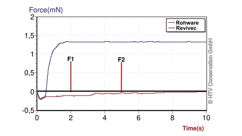
HTV has developed a process called revivec, which removes residues and oxide layers from electronic components. According to the manufacturer, the process can be used to safely and cost-effectively increase wetting forces and thus improve solderability.
Thanks to special cleaning formulations and the gentle effect of low-pressure plasma, it is possible to significantly improve the solderability of electronic components or printed circuit boards without chemical cleaning processes, which often form residues that cannot always be completely removed.
Due to the special composition of the plasma, the unwanted layers are broken up and removed. The selective effect on the surface only ensures that there is no risk to components or circuit boards. Even stubborn organic contaminants can be weakened in their bond by selective, gaseous cleaning formulations and then removed in a second process step.
Drying also takes place during cleaning, which is as gentle as vacuum drying at a reduced temperature. This means that no undesirable moisture is introduced, which could lead to the popcorn effect during assembly. The low-pressure process used cleans every corner of the component or PCB, even where conventional cleaning agents cannot reach. Depending on the level of contamination, the process can be parameterized in a multi-stage process and adapted with different gas formulations depending on the application.
Correct long-term storage
However, it makes more sense than cleaning components and PCBs after improper storage to maintain solderability through suitable storage processes and to stop the ageing processes. For this purpose, HTV has developed the TAB (thermal-absorptive gassing) storage process, which enables electronic components to be stored for up to 50 years while retaining their functionality and processability by avoiding or significantly reducing ageing processes. The main ageing processes are
- Diffusion processes (connections
and semiconductor chip) - Ageing due to moisture and oxygen
(corrosion and oxidation) - Ageing due to pollutants
- Whisker formation
- Tin plague
Conventional storage under nitrogen only reduces oxidation, which is only part of the ageing processes to be considered. In the so-called nitrogen dry packs, which are often used for long-term storage, there is still a small amount of oxygen in a standard packaging process, which means that oxidation processes cannot be ruled out. Other ageing processes, such as diffusion or corrosion caused by outgassing pollutants, are not reduced.
 Heavily contaminated component before and after treatment with revivec
The thermal-absorptive fumigation process is a combination of different methods and, in contrast to storage in nitrogen drypacks or corrosion protection films, reduces almost all relevant causes of ageing. This is essentially achieved by three mechanisms:
- The threshold of activation energy is increased by reducing the temperature. This means that chemical reactions do not take place at all or only very slowly. This virtually stops ageing processes, as can be clearly seen, for example, in the growth of the intermetallic phase (diffusion at the component connection) between the copper from the inside of the component pin and the tin on the pin surface. Other critical effects, such as tin plague, can also be avoided.
- A specially developed system of functional films and individually composed component-specific absorption materials: This ensures the absorption of organic and inorganic pollutants that outgas from the electronic components or diffuse into the packaging from the outside.
- A preservative gas cocktail surrounds the components to be stored and counteracts corrosion processes.
The components are also stored in high-security buildings, where they are protected against fire, theft and natural disasters.
Conclusion:
With the revivec process, the solderability of components and PCBs can be reliably improved, restoring the soldering process to the desired quality and avoiding costly failures. The TAB long-term preservation process makes it possible to maintain solderability for decades in advance during storage by avoiding or significantly reducing ageing processes.
