The expert seminar on assembly and joining technology featured twelve specialist presentations and an accompanying exhibition, as well as an intensive exchange of experiences to show which technologies are particularly promising for the future.
In addition to the partner companies ASM, ASYS, Christian Koenen, Stannol, Rehm, Vliesstoff Kasper and ZEVAC, other companies including ADL, kolb, MTM Ruhrzinn and Zestron took part in the 16th edition of this seminar series as exhibitors. Once again, the expert seminar was organized by Thorsten Schmidthausen (2ndMax) in Kirchheim, and as in previous years, Prof. Dr. Mathias Nowottnick, IEF/IGS of the University of Rostock, opened and moderated the event.
Avoiding soldering errors
Dr. Karin Hergert, Rehm Thermal Systems, explained what perfect soldered joints are and how they can be achieved in the first lecture entitled "Soldering on the way to perfection - avoiding soldering defects". Using examples of typical defects such as solder bridges, solder beads, component offset, component absence, non-soldering, tombstoning, wicking, graping and voids, she showed what is not perfect and how these defects can be detected. She also discussed the possible causes and corresponding preventative measures. Dr. Karin Hergert explained how adjustments to the soldering profile affect the error rates. There are often opposing effects here, for example, lower temperature gradients have a positive effect on tombstones, wicking and soldering beads but an unfavorable effect on graping.
Optimizing production
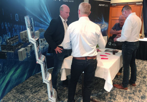 A lively exchange at the ASMPTAdrianTeuber and Fabian Autenrieth, ASYS Group, encouraged everyone to "Optimize Your Production" and used examples from production and its environment to illustrate how this can be achieved. The material and associated data flows are becoming increasingly complex due to the growing diversity in electronics, which leads to larger and confusing warehouses, long distances and other problems. Using the milk run principle, magazine and reel handling use cases, they demonstrated that logistics automation based on software tools is a solution. Even the changeover of the paste printer (EKRA Serio 6000) and the entire SMT line to a new product can now be fully automated thanks to modern tools, with everything being logged and production data being exchanged with the control system. These new possibilities are based on an alliance of manufacturers whose machines and production support systems are capable of Pulse PRO line management thanks to standardized interfaces. The Pulse PRO concept offers simple, bidirectional communication via the integrated messenger system, remote monitoring for critical processes using a freely positionable camera for transmitting live videos to mobile devices, complete machine information such as serial number, software version and contact to the support hotline at a glance, as well as access-protected file storage for the central storage of machine-specific documents. Adrian Teuber and Fabian Autenrieth recommended taking a step-by-step approach to optimizing production.
Reducing theCO2 footprint with soldering agents
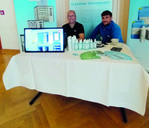 Kolb presented its range of cleaning systems and chemicals for electronics productionMarcoDörr from Stannol used the company's history to show how selecting the right soldering agents can reduce the carbon footprint in electronics production and what needs to be considered when making the switch. Stannol developed the first sustainable solder wire back in 2014, followed by the development of the Fairtin criteria in 2018 and in 2020, a completely 'green' product portfolio was introduced under the name 'greenconnect', which focuses on the aspect of sustainability. The company is now in the process of drawing up its first carbon footprint.
Marco Dörr began by comparing water-based and solvent-based fluxes. The former are not a drop-in solution, as water requires significantly more heat for evaporation, i.e. longer and higher preheating in the soldering system, which is associated with a higher temperature load for the components. Nevertheless, they have a much better CO2 footprint. In addition, transportation costs and the purchase of water-based fluxes are cheaper. With Solar PV EF160 Bio PV, Stannol has now launched a new flux on the market which, unlike previous alcohol-based fluxes, is 95% bio-based and therefore almost CO2 emission-free. Following an insight into global tin consumption, Marco Dörr discussed the reuse of tin from waste. This is not a problem, as there is no analytical difference between recycled and primary tin. Primary tin emits 2.18 tons of CO2 per ton of Sn, whereas secondary tin emits only 0.024 tons of CO2, i.e. 98.9% less. It was recommended to use water-based fluxes for wave and selective soldering and to operate the systems with green electricity. Otherwise, organic ethanol-based fluxes should be used. Fairtin and Greenconnect products are sustainable.
Low temperature soldering reduces the heat requirement
As Helge Schimanski, Fraunhofer ISIT, Itzehoe, explained, low-melting solders can have advantages in soldering. This is because open solder joints can be avoided, which can occur with the higher soldering temperatures of the SAC reflow soldering process due to the different coefficients of thermal expansion (CTE) of the PCB and components as a result of warping. The warping effect is less pronounced when soldering at lower temperatures. However, low temperature soldering (LTS) with SnBiX solders is only possible if it is suitable for the operating temperatures of the electronics. LTS tests with a selection of components showed no significant differences in wetting or in the properties of the resulting solder joints compared with SAC. Depending on the LTS solder paste used, the stencil openings may need to be adjusted, as Helge Schimanski explained using an example.
The basis of digitalization and new technological challenges
 A good mood prevailed at the Ruhrzinn standDigitalinformation is nothing new. It has been around for 3.5 billion years in the form of quaternary-coded genetic information, the DNA double helix. Prof. Dr. Mathias Nowottnick, IEF/IGS at the University of Rostock, used a series of image examples to show how the technology has developed. The technological basis of digitization begins with the ancient calculating machine of Antikythera. The first product of modern times is the mechanical calculating machine invented by Gottfried Wilhelm Leibniz in 1673. The first printing calculator was invented around 1905 and the first pocket calculator in 1920. The first functional digital computer was designed by Konrad Zuse and Helmut Schreyer in 1941. After that, things got faster and faster, driven by semiconductor technology - integrated circuits were invented in 1959. Intel introduced the 8-bit microprocessor with approx. 3500 transistors in 1972 and Gordon Moore predicted in 1975 that the complexity of integrated circuits would double every two years, which has been confirmed. In the meantime, structures in the nanometre range and 3D structures have been realized in the semiconductor sector, and miniaturization and integration in other areas of electronics has also made great progress, e.g. up to smart sensors and actuators in microsystems technology. Now the development is moving towards quantum computers. However, the technological challenges are enormous. And new products and applications also include new solders, microfluidics and electro-optical printed circuit boards.
Rapid realization of the IIoT through retrofitting
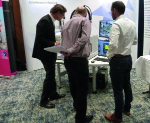 The demonstration of the ONYX machine from ZEVAC aroused interestDigitalization is only progressing slowly in production. The reasons for this include the large amount of older equipment that is not designed for the IIoT, the heterogeneous machine and process landscape and no or insufficient personnel with IIoT expertise. Christian Groß from the company in.hub called for the rapid implementation of IIoT - industrial digitalization in the here and now - tomorrow could be too late. He discussed the products his company has available for this. in.hub is an IIoT specialist for condition monitoring with a focus on retrofitting for recording, networking and integration into cloud or server-based IT systems. Christian Groß showed that retrofitting is a key factor in digitalization. This is because retrofitting with smart sensors and interfaces for networking across various protocols makes it possible to integrate existing production facilities into modern networks and systems and thus realize the IIoT. This enables the goal of products controlling production to be achieved. Setting up the IIoT operating systems should be as simple as possible and possible for everyone, i.e. smartphone-like. Characteristics of modern products for the realization of the digital factory are therefore open platforms where the customer can decide what and how to use. This includes easy access to expert tools and a marketplace with suitable applications for every task that are easy to install and use.
Conformal coating to protect the printed circuit board
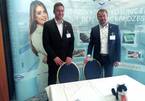 Christian KoenenDr.Gerald Katzler from Nidec DriveXpert gave an overview of the requirements and possibilities of conformal coating - new developments in PCB protection - as well as advice on the selection and application of the coating. The protection task should be precisely defined, as this (largely) specifies the coating. And every coating (type) has its strengths and applications. Cleaning the PCBs improves adhesion and reduces delamination. Without cleaning, UV-curing elastomers show the lowest tendency to defects. The formation of bubbles depends on the layout and the coating application. This can be applied by spraying, jetting or dispensing, depending on the coating plan and viscosity. UV-curing paints have advantages, including 100% solids content, no/low VOC content and touch-resistant immediately after UV irradiation - final curing within seven days. For the motor control application, Nidec has chosen a UV-curable elastomer coating with a faster secondary curing mechanism and application with a jet system, so that the coated circuit boards can be processed directly and production space is saved.
Low-pressure sintering of silver contacts
Dr. Jörg Meyer, TU Dresden, reported on the technology development for reliable low-pressure silver sintered contacts and presented results from the AgLowPress funding project. This served to develop processes and technology, including an R&D system for the force-controlled low-pressure sintering of silver sinter contacts for power electronics. The test setups and procedures as well as the results of the sintering tests achieved were described in detail (e.g. influences on the porosity of the sintered joint). The force-controlled sintering system for low pressure is now ready for operation: budatec SP300 for 0.5 to 300kN, at max. 350°C, with N2, H2). The tests were carried out with an application-oriented test setup with large process variation. A pressure in the range of 5 to 10Mpa for 2 to 5min and a temperature of 250°C is recommended for sintering. Further findings are that a lower temperature can be compensated by higher pressure and that the influence of sintering time in the considered range (2 to 10 min) is low. Furthermore, a correlation was found between the process parameters and the shear strength.
Digitalization of pump production
Stefan Lau, Wilo Group Electronics & Motors, provided information on the digitalization of production and work processes in intelligent pump manufacturing using the example of his company and its experiences.
Self-validation of critical electronics
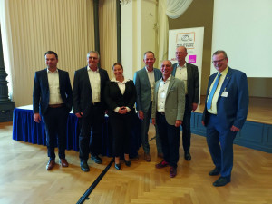 Prof. Dr. Mathias Nowottnick (far right) with speakersUsingthe funded project SesiM (self-validation of complex electronic systems in safety-critical mobility applications based on greybox models), Klaus Wilke, Siemens Technology Berlin, explained how the self-validation of electronics in safety-critical applications (automotive and railroad technology) can be implemented to ensure functional integrity based on computational intelligence and machine learning. Data from development and production as well as operating and load data in the field are required for the comprehensive system description. A data flow for the entire life cycle must be developed for system optimization and the Built-In-Self-Test (BIST) for system diagnostics. The data is evaluated using a hybrid system model for condition monitoring and self-validation and using AI to ensure reliability and protection against manipulation. This also results in new requirements for the data for quality assurance in production, i.e. for SPI, AOI and AXI. Reliability-relevant data must also be recorded and data quality improved, including pin-specific data allocation. It is also necessary to develop accelerated environmental tests on test setups and online parameter monitoring as well as methods for combined stress tests. Complex electronic systems can be divided into reliability-relevant blocks for modeling according to the functional structure, so that a synthesis of the overall system and interaction of the functional blocks is possible for testing and simulation. Anomaly detection, i.e. an algorithm for detecting spontaneous and creeping deviations, is also required. Klaus Wilke used examples to illustrate how this can be implemented in practice and also discussed the service life forecast based on the assembly data, the system model and the quality data from production.
Approaches to optimizing precision printing
Based on current market data and technology trends, Michael Brianda from Christian Koenen presented tried-and-tested optimization proposals for fine pitch stencil printing. Unevenness on the substrate, e.g. due to high solder resist, is often a challenge for fine pitch printing. Substrate misalignment, incorrect pad sizes and bending also cause problems with paste printing. Bending can be avoided with PCB supports, but unfavorably positioned supports promote bridging and caution is required in the vicinity of components. Milled stepped stencils, a technique patented by Christian Koenen, can be used to apply paste at different heights and thus optimize the paste volume. The release behavior can be improved with plasma treatment. Squeegee angle and speed influence the filling of the openings with solder paste. Material and tool selection as well as the appropriate parameters are decisive for precision printing.
Sintering technology for power modules
In the final lecture, Prof. Hans-Jürgen Albrecht from budatec discussed the possibility of the 'Application of Sintering Technology for Power Modules' and gave an overview of the international status of sintering technology and its development. He compared Ag sintering with Cu sintering and these with alternative joining technologies such as TLPS in terms of meeting reliability requirements and processing. Prof. Hans-Jürgen Albrecht presented the results of corresponding analyses in the form of numerous images and diagrams. The results show that silver and copper sinter pastes can be used in power modules as a substitute for high-lead solder using today's sintering technology. The service life of the sintered joints realized with this technology proved to be many times longer in cycle tests and the processability is acceptable.
www.wir-gehen-in-die-tiefe.de www.2ndmax.de


